X28HC64J-12 Intersil, X28HC64J-12 Datasheet - Page 3
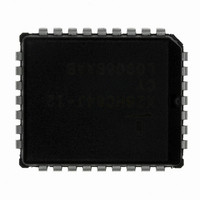
X28HC64J-12
Manufacturer Part Number
X28HC64J-12
Description
IC EEPROM 64KBIT 120NS 32PLCC
Manufacturer
Intersil
Datasheet
1.X28HC64D-12.pdf
(17 pages)
Specifications of X28HC64J-12
Format - Memory
EEPROMs - Parallel
Memory Type
EEPROM
Memory Size
64K (8K x 8)
Speed
120ns
Interface
Parallel
Voltage - Supply
4.5 V ~ 5.5 V
Operating Temperature
0°C ~ 70°C
Package / Case
32-LCC (J-Lead)
Lead Free Status / RoHS Status
Contains lead / RoHS non-compliant
Available stocks
Company
Part Number
Manufacturer
Quantity
Price
Company:

Part Number:
X28HC64J-12
Manufacturer:
XICOR
Quantity:
3 198
Company:
Part Number:
X28HC64J-12
Manufacturer:
XICOR
Quantity:
5 510
Part Number:
X28HC64J-12
Manufacturer:
XICOR
Quantity:
20 000
Company:
Part Number:
X28HC64J-12T1
Manufacturer:
INTERSIL
Quantity:
4 219
Part Number:
X28HC64J-12TZ
Manufacturer:
INTERSIL
Quantity:
20 000


A
ADDRESS
INPUTS
Pin Descriptions
Addresses (A
The Address inputs select an 8-bit memory location during a
read or write operation.
Chip Enable (CE)
The Chip Enable input must be LOW to enable all read/write
operations. When CE is HIGH, power consumption is reduced.
Output Enable (OE)
The Output Enable input controls the data output buffers and
is used to initiate read operations.
Data In/Data Out (I/O
Data is written to or read from the X28HC64 through the I/O
pins.
Write Enable (WE)
The Write Enable input controls the writing of data to the
X28HC64.
Block Diagram
0
–A
12
V
V
OE
WE
CE
CC
SS
SYMBOL
I/O
A
V
V
0
WE
OE
NC
CE
0
-A
CC
SS
-I/O
0
12
-A
7
LATCHES AND
12
TABLE 1. PIN NAMES
X BUFFERS
LOGIC AND
DECODER
Y BUFFERS
CONTROL
DECODER
LATCHES
TIMING
)
AND
0
-I/O
7
3
)
Data Input/Output
DESCRIPTION
Address Inputs
Output Enable
Write Enable
Chip Enable
No Connect
DATA INPUTS/OUTPUTS
Ground
+5V
AND LATCHES
I/O BUFFERS
65,536-BIT
I/O
EEPROM
ARRAY
0
–I/O
7
X28HC64
Device Operation
Read
Read operations are initiated by both OE and CE LOW. The
read operation is terminated by either CE or OE returning
HIGH. This two line control architecture eliminates bus
contention in a system environment. The data bus will be in
a high impedance state when either OE or CE is HIGH.
Write
Write operations are initiated when both CE and WE are
LOW and OE is HIGH. The X28HC64 supports both a CE
and WE controlled write cycle. That is, the address is latched
by the falling edge of either CE or WE, whichever occurs
last. Similarly, the data is latched internally by the rising edge
of either CE or WE, whichever occurs first. A byte write
operation, once initiated, will automatically continue to
completion, typically within 2ms.
Page Write Operation
The page write feature of the X28HC64 allows the entire
memory to be written in 0.25 seconds. Page write allows two
to sixty-four bytes of data to be consecutively written to the
X28HC64 prior to the commencement of the internal
programming cycle. The host can fetch data from another
device within the system during a page write operation
(change the source address), but the page address (A
through A
during this operation must be the same as the initial page
address.
The page write mode can be initiated during any write
operation. Following the initial byte write cycle, the host can
write an additional one to sixty-three bytes in the same
manner. Each successive byte load cycle, started by the WE
HIGH to LOW transition, must begin within 100µs of the
falling edge of the preceding WE. If a subsequent WE HIGH
to LOW transition is not detected within 100µs, the internal
automatic programming cycle will commence. There is no
page write window limitation. Effectively the page write
window is infinitely wide, so long as the host continues to
access the device within the byte load cycle time of 100µs.
Write Operation Status Bits
The X28HC64 provides the user two write operation status
bits. These can be used to optimize a system write cycle
time. The status bits are mapped onto the I/O bus as shown
in Figure 1.
I/O
12
DP
) for each subsequent valid write cycle to the part
FIGURE 1. STATUS BIT ASSIGNMENT
TB
5
4
TOGGLE BIT
DATA POLLING
RESERVED
3
2
1
August 28, 2009
0
6
FN8109.2
Related parts for X28HC64J-12
Image
Part Number
Description
Manufacturer
Datasheet
Request
R

Part Number:
Description:
Intersil Corporation [CMOS Serial Controller Interface]
Manufacturer:
Intersil Corporation
Datasheet:
Part Number:
Description:
Manufacturer:
Intersil Corporation
Datasheet:
Part Number:
Description:
357-036-542-201 CARDEDGE 36POS DL .156 BLK LOPRO
Manufacturer:
Intersil Corporation
Datasheet:
Part Number:
Description:
1024-Word x 4-Bit LSI Static RAM
Manufacturer:
Intersil Corporation
Datasheet:
Part Number:
Description:
General Purpose NPN Transistor Arrays FN341.4
Manufacturer:
Intersil Corporation
Datasheet:
Part Number:
Description:
CMOS 16-Bit Microprocessor
Manufacturer:
Intersil Corporation
Datasheet:
Part Number:
Description:
Manufacturer:
Intersil Corporation
Datasheet:
Part Number:
Description:
Manufacturer:
Intersil Corporation
Datasheet:
Part Number:
Description:
Manufacturer:
Intersil Corporation
Datasheet:
Part Number:
Description:
Manufacturer:
Intersil Corporation
Datasheet:
Part Number:
Description:
CMOS 6-Bit Latch and Decoder Memory Interfaces
Manufacturer:
Intersil Corporation
Datasheet:
Part Number:
Description:
CA3046General Purpose NPN Transistor Arrays
Manufacturer:
Intersil Corporation
Datasheet:
Part Number:
Description:
Manufacturer:
Intersil Corporation
Datasheet:
Part Number:
Description:
TR909 DLC/FLC SLIC with Low Power Standby
Manufacturer:
Intersil Corporation
Datasheet:
Part Number:
Description:
Manufacturer:
Intersil Corporation
Datasheet: