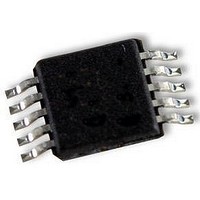
LM5106MM National Semiconductor, LM5106MM Datasheet - Page 4

LM5106MM
Manufacturer Part Number
LM5106MM
Description
DRIVER, MOSFET, HALF BRIDGE, SMD
Manufacturer
National Semiconductor
Datasheet
1.LM5106MM.pdf
(12 pages)
Specifications of LM5106MM
Device Type
Half Bridge
Module Configuration
Half Bridge
Peak Output Current
1.8A
Input Delay
115ns
Output Delay
32ns
Supply Voltage Range
8V To 14V
Driver Case Style
MSOP
No. Of Pins
10
Lead Free Status / RoHS Status
Lead free / RoHS Compliant
Available stocks
Company
Part Number
Manufacturer
Quantity
Price
Company:
Part Number:
LM5106MM
Manufacturer:
TI
Quantity:
24 480
Company:
Part Number:
LM5106MM
Manufacturer:
OKISEMICONDUCTOR
Quantity:
4 879
Company:
Part Number:
LM5106MMX
Manufacturer:
TI
Quantity:
24 480
Part Number:
LM5106MMX
Manufacturer:
TI/德州仪器
Quantity:
20 000
Part Number:
LM5106MMX/NOPB
Manufacturer:
TI/德州仪器
Quantity:
20 000
www.national.com
t
t
t
t
t
t
t
DT1, DT2
MDT
t
t
LPHL
HPHL
LPLH
HPLH
LPLH
HPLH
en
R
F
Switching Characteristics
type apply over the full operating junction temperature range. Unless otherwise specified, V
Load on LO or HO
Note 1: Absolute Maximum Ratings indicate limits beyond which damage to the component may occur. Operating Ratings are conditions under which operation
of the device is guaranteed. Operating Ratings do not imply guaranteed performance limits. For guaranteed performance limits and associated test conditions,
see the Electrical Characteristics tables.
Note 2: The human body model is a 100 pF capacitor discharged through a 1.5kΩ resistor into each pin. Pin 2, Pin 3 and Pin 4 are rated at 500V.
Note 3: 4 layer board with Cu finished thickness 1.5/1.0/1.0/1.5 oz. Maximum die size used. 5x body length of Cu trace on PCB top. 50 x 50mm ground and
power planes embedded in PCB. See Application Note AN-1187.
Note 4: Min and Max limits are 100% production tested at 25°C. Limits over the operating temperature range are guaranteed through correlation using Statistical
Quality Control (SQC) methods. Limits are used to calculate National’s Average Outgoing Quality Level (AOQL).
Note 5: The θ
Note 6: In the application the HS node is clamped by the body diode of the external lower N-MOSFET, therefore the HS voltage will generally not exceed -1V.
However in some applications, board resistance and inductance may result in the HS node exceeding this stated voltage transiently.
If negative transients occur on HS, the HS voltage must never be more negative than V
not exceed -5V.
Symbol
, t
sd
JA
Lower Turn-Off Propagation Delay
Upper Turn-Off Propagation Delay
Lower Turn-On Propagation Delay
Upper Turn-On Propagation Delay
Lower Turn-On Propagation Delay
Upper Turn-On Propagation Delay
Enable and Shutdown propagation delay
Dead-time LO OFF to HO ON & HO OFF to LO
ON
Dead-time matching
Either Output Rise Time
Either Output Fall Time
is not a constant for the package and depends on the printed circuit board design and the operating conditions.
(Note
4).
Parameter
Specifications in standard typeface are for T
RDT = 100k
RDT = 100k
RDT = 10k
RDT = 10k
RDT = 100k
RDT = 10k
RDT = 100k
C
C
L
L
= 1000pF
= 1000pF
4
Conditions
DD
- 15V. For example, if V
J
Min
400
450
= +25°C, and those in boldface
DD
85
85
DD
= 10V, the negative transients at HS must
= HB = 12V, V
Typ
520
570
115
115
510
32
32
36
86
50
15
10
SS
Max
640
690
160
160
56
56
= HS = 0V, No
Units
ns
ns
ns
ns
ns
ns
ns
ns
ns
ns
ns
ns


