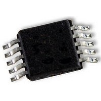
LM5106MM National Semiconductor, LM5106MM Datasheet - Page 8

LM5106MM
Manufacturer Part Number
LM5106MM
Description
DRIVER, MOSFET, HALF BRIDGE, SMD
Manufacturer
National Semiconductor
Datasheet
1.LM5106MM.pdf
(12 pages)
Specifications of LM5106MM
Device Type
Half Bridge
Module Configuration
Half Bridge
Peak Output Current
1.8A
Input Delay
115ns
Output Delay
32ns
Supply Voltage Range
8V To 14V
Driver Case Style
MSOP
No. Of Pins
10
Lead Free Status / RoHS Status
Lead free / RoHS Compliant
Available stocks
Company
Part Number
Manufacturer
Quantity
Price
Company:
Part Number:
LM5106MM
Manufacturer:
TI
Quantity:
24 480
Company:
Part Number:
LM5106MM
Manufacturer:
OKISEMICONDUCTOR
Quantity:
4 879
Company:
Part Number:
LM5106MMX
Manufacturer:
TI
Quantity:
24 480
Part Number:
LM5106MMX
Manufacturer:
TI/德州仪器
Quantity:
20 000
Part Number:
LM5106MMX/NOPB
Manufacturer:
TI/德州仪器
Quantity:
20 000
www.national.com
Operational Notes
The LM5106 is a single PWM input Gate Driver with Enable
that offers a programmable dead-time. The dead-time is set
with a resistor at the RDT pin and can be adjusted from 100ns
to 600ns. The wide dead-time programming range provides
the flexibility to optimize drive signal timing for a wide range
of MOSFETS and applications.
The RDT pin is biased at 3V and current limited to 1 mA max-
imum programming current. The time delay generator will
accommodate resistor values from 5k to 100k with a dead-
time time that is proportional to the RDT resistance. Ground-
ing the RDT pin programs the LM5106 to drive both outputs
with minimum dead-time.
STARTUP AND UVLO
Both top and bottom drivers include under-voltage lockout
(UVLO) protection circuitry which monitors the supply voltage
(V
dently. The UVLO circuit inhibits each driver until sufficient
supply voltage is available to turn-on the external MOSFETs,
and the UVLO hysteresis prevents chattering during supply
voltage transitions. When the supply voltage is applied to the
V
until V
Any UVLO condition on the bootstrap capacitor will disable
only the high side output (HO).
LAYOUT CONSIDERATIONS
The optimum performance of high and low side gate drivers
cannot be achieved without taking due considerations during
circuit board layout. The following points are emphasized:
1.
2.
3.
4.
DD
DD
pin of the LM5106, the top and bottom gates are held low
) and bootstrap capacitor voltage (HB – HS) indepen-
Low ESR / ESL capacitors must be connected close to
the IC between VDD and VSS pins and between HB and
HS pins to support high peak currents being drawn from
VDD and HB during the turn-on of the external
MOSFETs.
To prevent large voltage transients at the drain of the top
MOSFET, a low ESR electrolytic capacitor and a good
quality ceramic capacitor must be connected between
the MOSFET drain and ground (VSS).
In order to avoid large negative transients on the switch
node (HS) pin, the parasitic inductances between the
source of the top MOSFET and the drain of the bottom
MOSFET (synchronous rectifier) must be minimized.
Grounding considerations:
a) The first priority in designing grounding connections is
to confine the high peak currents that charge and
discharge the MOSFET gates to a minimal physical area.
This will decrease the loop inductance and minimize
noise issues on the gate terminals of the MOSFETs. The
gate driver should be placed as close as possible to the
MOSFETs.
b) The second consideration is the high current path that
includes the bootstrap capacitor, the bootstrap diode, the
local ground referenced bypass capacitor, and the low
side MOSFET body diode. The bootstrap capacitor is
DD
exceeds the UVLO threshold, typically about 6.9V.
FIGURE 4. LM5106 Enable: t
20175930
sd
8
5.
POWER DISSIPATION CONSIDERATIONS
The total IC power dissipation is the sum of the gate driver
losses and the bootstrap diode losses. The gate driver losses
are related to the switching frequency (f), output load capac-
itance on LO and HO (C
be roughly calculated as:
There are some additional losses in the gate drivers due to
the internal CMOS stages used to buffer the LO and HO out-
puts. The following plot shows the measured gate driver
power dissipation versus frequency and load capacitance. At
higher frequencies and load capacitance values, the power
dissipation is dominated by the power losses driving the out-
put loads and agrees well with the above equation. This plot
can be used to approximate the power losses due to the gate
drivers.
HS TRANSIENT VOLTAGES BELOW GROUND
The HS node will always be clamped by the body diode of the
lower external FET. In some situations, board resistances and
inductances can cause the HS node to transiently swing sev-
eral volts below ground. The HS node can swing below
ground provided:
recharged on a cycle-by-cycle basis through the
bootstrap diode from the ground referenced VDD bypass
capacitor. The recharging occurs in a short time interval
and involves high peak current. Minimizing this loop
length and area on the circuit board is important to ensure
reliable operation.
The resistor on the RDT pin must be placed very close
to the IC and separated from the high current paths to
avoid noise coupling to the time delay generator which
could disrupt timer operation.
Gate Driver Power Dissipation (LO + HO)
FIGURE 5. LM5106 Dead-time: DT
P
DGATES
L
V
), and supply voltage (V
= 2 • f • C
CC
= 12V
L
• V
DD
2
DD
20175905
) and can
20175931


