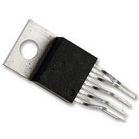
LM4950TS National Semiconductor, LM4950TS Datasheet - Page 17

LM4950TS
Manufacturer Part Number
LM4950TS
Description
Audio Power Amplifier IC
Manufacturer
National Semiconductor
Datasheet
1.LM4950TS.pdf
(25 pages)
Specifications of LM4950TS
Amplifier Case Style
TO-220
No. Of Pins
9
Peak Reflow Compatible (260 C)
No
Termination Type
Through Hole
Leaded Process Compatible
No
Package / Case
9-TO-220
Operational Class
Class-AB
Audio Amplifier Function
Speaker
Input Offset Voltage
30@12VmV
Total Harmonic Distortion
0.05@4Ohm@2.5W%
Single Supply Voltage (typ)
12/15V
Dual Supply Voltage (typ)
Not RequiredV
Power Supply Requirement
Single
Rail/rail I/o Type
No
Power Supply Rejection Ratio
70dB
Single Supply Voltage (min)
9.6V
Single Supply Voltage (max)
16V
Dual Supply Voltage (min)
Not RequiredV
Dual Supply Voltage (max)
Not RequiredV
Operating Temp Range
-40C to 85C
Operating Temperature Classification
Industrial
Mounting
Surface Mount
Pin Count
9 +Tab
Package Type
TO-263
Lead Free Status / RoHS Status
Contains lead / RoHS non-compliant
Lead Free Status / RoHS Status
Contains lead / RoHS non-compliant
Available stocks
Company
Part Number
Manufacturer
Quantity
Price
Part Number:
LM4950TS
Manufacturer:
NS/国半
Quantity:
20 000
Company:
Part Number:
LM4950TSX
Manufacturer:
INTEL
Quantity:
182
Part Number:
LM4950TSX
Manufacturer:
NS/国半
Quantity:
20 000
Application Information
SELECTING EXTERNAL COMPONENTS
Input Capacitor Value Selection
Two quantities determine the value of the input coupling
capacitor: the lowest audio frequency that requires amplifi-
cation and desired output transient suppression.
As shown in Figure 3, the input resistor (R
capacitor (C
that is found using Equation (7).
As an example when using a speaker with a low frequency
limit of 50Hz, C
C
efficiency, full range speaker whose response extends below
30Hz.
Bypass Capacitor Value
Besides minimizing the input capacitor size, careful consid-
eration should be paid to value of C
connected to the BYPASS pin. Since C
how fast the LM4950 settles to quiescent operation, its value
is critical when minimizing turn-on pops. The slower the
LM4950’s outputs ramp to their quiescent DC voltage (nomi-
nally V
equal to 10µF along with a small value of C
0.1µF to 0.39µF), produces a click-less and pop-less shut-
down function. As discussed above, choosing C
than necessary for the desired bandwidth helps minimize
clicks and pops.
OPTIMIZING CLICK AND POP REDUCTION
PERFORMANCE
The LM4950 contains circuitry that eliminates turn-on and
shutdown transients ("clicks and pops"). For this discussion,
turn-on refers to either applying the power supply voltage or
when the micro-power shutdown mode is deactivated.
As the V
final value, the LM4950’s internal amplifiers are configured
as unity gain buffers and are disconnected from the AMP
and AMP
pacitor connected between the BYPASS pin and GND in a
INA
shown in Figure 3 allows the LM4950 to drive high
DD
DD
/2), the smaller the turn-on pop. Choosing C
B
/2 voltage present at the BYPASS pin ramps to its
pins. An internal current source charges the ca-
IN
) produce a high pass filter cutoff frequency
i
, using Equation (7) is 0.159µF. The 0.39µF
f
c
= 1/2πR
i
C
i
BYPASS
BYPASS
(Continued)
IN
IN
) and the input
, the capacitor
(in the range of
IN
determines
no larger
BYPASS
(7)
A
17
controlled manner. Ideally, the input and outputs track the
voltage applied to the BYPASS pin. The gain of the internal
amplifiers remains unity until the voltage applied to the BY-
PASS pin.
The gain of the internal amplifiers remains unity until the
voltage on the bypass pin reaches V
voltage on the bypass pin is stable, the device becomes fully
operational and the amplifier outputs are reconnected to
their respective output pins. Although the BYPASS pin cur-
rent cannot be modified, changing the size of C
the device’s turn-on time. Here are some typical turn-on
times for various values of C
In order eliminate "clicks and pops", all capacitors must be
discharged before turn-on. Rapidly switching V
allow the capacitors to fully discharge, which may cause
"clicks and pops".
There is a relationship between the value of C
C
is applied or the shutdown mode is deactivated. Best perfor-
mance is achieved by setting the time constant created by
C
given value of C
DRIVING PIEZO-ELECTRIC SPEAKER TRANSDUCERS
The LM4950 is able to drive capacitive piezo-electric trans-
ducer loads that are less than equal to 200nF. Stable opera-
tion is assured by placing 33pF capacitors in parallel with the
20kΩ feedback resistors. The additional capacitors are
shown in Figure 4.
When driving piezo-electric tranducers, sound quality and
accoustic power is entirely dependent upon a transducer’s
frequency response and efficiency. In this application, power
dissipated by the LM4950 is very low, typically less than
250mW when driving a 200nF piezo-electric transduce
(V
BYPASS
IN
DD
and R
= 12V).
that ensures minimum output transient when power
i
C
+ R
B
1.0
2.2
4.7
10
(µF)
f
BYPASS
to a value less than the turn-on time for a
as shown in the table above.
BYPASS
:
DD
T
/2. As soon as the
ON
120
120
200
440
(ms)
BYPASS
DD
www.national.com
may not
IN
alters
and


