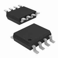
AD22151YR-REEL Analog Devices Inc, AD22151YR-REEL Datasheet - Page 3

AD22151YR-REEL
Manufacturer Part Number
AD22151YR-REEL
Description
IC MAGNETIC FIELD SNSR LIN 8SOIC
Manufacturer
Analog Devices Inc
Type
Linear - Unipolar, Bipolarr
Datasheet
1.AD22151YRZ.pdf
(8 pages)
Specifications of AD22151YR-REEL
Rohs Status
RoHS non-compliant
Sensing Range
Unlimited
Voltage - Supply
4.5 V ~ 6 V
Current - Supply
10mA
Current - Output (max)
15mA
Output Type
Analog, Ratiometric
Operating Temperature
-40°C ~ 150°C
Package / Case
8-SOIC (0.154", 3.90mm Width)
Features
-
CIRCUIT OPERATION
The AD22151 consists of epi Hall plate structures located at the
center of the die. The Hall plates are orthogonally sampled by
commutation switches via a differential amplifier. The two
amplified Hall signals are synchronously demodulated to provide a
resultant offset cancellation (see Figure 3). The demodulated
signal passes through a noninverting amplifier to provide final
gain and drive capability. The frequency at which the output
signal is refreshed is 50 kHz.
TEMPERATURE DEPENDENCIES
The uncompensated gain temperature coefficient (G
AD22151 is the result of fundamental physical properties asso-
ciated with silicon bulk Hall plate structures. Low doped Hall
plates operated in current bias mode exhibit a temperature
relationship determined by the action of scattering mechanisms
and doping concentration.
The relative value of sensitivity to magnetic field can be altered
by the application of mechanical force upon silicon. The mecha-
nism is principally the redistribution of electrons throughout the
REV. A
Figure 3. Relative Quiescent Offset vs. Temperature
–0.001
–0.002
–0.003
–0.004
0.005
0.004
0.003
0.002
0.001
0
140
120
*SHADED AREA REPRESENTS
GND
TC1
TC2
TC3
MAGNETIC FIELD AREA OF
SENSITIVITY (20MILS
POSITIVE B FIELD INTO TOP OF
PACKAGE RESULTS IN A POSITIVE
VOLTAGE RESPONSE
PIN CONFIGURATION
100
AREA OF SENSITIVITY*
1
2
3
4
1
2
3
4
(Not to Scale)
(Not to Scale)
AD22151
TOP VIEW
80
TEMPERATURE – C
60
8
7
6
5
8
7
6
5
20MILS)
40
REF
GAIN
OUTPUT
V
CC
20
0
–20
TCU
) of the
–40
–3–
Pin No.
1
2
3
4
5
6
7
8
“valleys” of the silicon crystal. Mechanical force on the sensor is
attributable to package-induced stress. The package material
acts to distort the encapsulated silicon, altering the Hall cell
gain by ± 2% and G
Figure 4 shows the typical G
This is the observable alteration of gain with respect to tempera-
ture with Pin 3 (TC3) held at a constant 2.5 V (uncompensated).
If a permanent magnet source used in conjunction with the
sensor also displays an intrinsic TC (B
into the total temperature compensation of the sensor assembly.
Figures 5 and 6 represent typical overall temperature/gain per-
formance for a sensor and field combination (B
Figure 5 is the total drift in volts over a –40∞C to +150∞C tem-
perature range with respect to applied field. Figure 6 represents
typical percentage gain variation from 25∞C. Figures 7 and 8
show similar data for a B
Figure 4. Uncompensated Gain Variation (from
25 ∞ C) vs. Temperature
14
12
10
–2
–4
–6
8
6
4
2
0
–40
Description
Temperature Compensation 1
Temperature Compensation 2
Temperature Compensation 3
Ground
Output
Gain
Reference
Positive Power Supply
PIN FUNCTION DESCRIPTIONS
TCU
10
by ± 200 ppm.
TC
TEMPERATURE – C
TCU
= –2000 ppm.
characteristic of the AD22151.
60
TC
), it will require factoring
110
AD22151
TC
Connection
Output
Output
Input/Output
Output
Input
Output
= –200 ppm).
160


