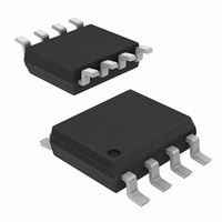
AD22151YR-REEL Analog Devices Inc, AD22151YR-REEL Datasheet - Page 5

AD22151YR-REEL
Manufacturer Part Number
AD22151YR-REEL
Description
IC MAGNETIC FIELD SNSR LIN 8SOIC
Manufacturer
Analog Devices Inc
Type
Linear - Unipolar, Bipolarr
Datasheet
1.AD22151YRZ.pdf
(8 pages)
Specifications of AD22151YR-REEL
Rohs Status
RoHS non-compliant
Sensing Range
Unlimited
Voltage - Supply
4.5 V ~ 6 V
Current - Supply
10mA
Current - Output (max)
15mA
Output Type
Analog, Ratiometric
Operating Temperature
-40°C ~ 150°C
Package / Case
8-SOIC (0.154", 3.90mm Width)
Features
-
to self-heating as a function of power dissipation. Second, pack-
age stress effect alters the specific operating parameters of the
gain compensation, particularly the specific crossover tempera-
ture of TC1, TC3 (
CONFIGURATION AND COMPONENT SELECTION
There are three areas of sensor operation that require external
component selection: temperature compensation (R1), signal
gain (R2 and R3), and offset (R4).
Temperature
If the internal gain compensation is used, an external resistor is
required to complete the gain TC circuit at Pin 3. A number of
factors contribute to the value of this resistor:
a. The intrinsic Hall cell sensitivity TC
b. Package induced stress variation in a.
c. Specific field TC
d. R1, TC.
The final value of target compensation also dictates the use of
either Pin 1 or Pin 2. Pin 1 is provided to allow for large nega-
tive field TC devices such as ferrite magnets; thus, R1 would be
connected to Pins 1 and 3.
Pin 2 uses an internal resistive TC to optimize smaller field
coefficients such as Alnico down to 0 ppm coefficients when
only the sensor gain TC itself is dominant. Because the TC of
R1 itself will also affect the compensation, a low TC resistor
(± 50 ppm) is recommended.
Figures 10 and 11 indicate R1 resistor values and their associ-
ated effectiveness for Pins 1 and 2, respectively. Note that the
indicated drift response in both cases incorporates the intrinsic
Hall sensitivity TC (B
For example, the AD22151 sensor is to be used in conjunction
with an Alnico material permanent magnet. The TC of such mag-
nets is
that a compensating drift of 200 ppm at Pin 3 requires a nomi-
nal value of R1 = 18 kW (assuming negligible drift of R1 itself).
REV. A
(Ferrite), 0 ppm (electromagnet), and so on.
Figure 10. Drift Compensation (Pins 1 and 3) vs.
Typical Resistor Value R1
3000
1500
3500
2500
2000
1000
500
0
–200 ppm (see Figures 5 and 6). Figure 11 indicates
0
5
TCU
± 10∞C).
–200 ppm (Alnico), –2000 ppm
10
).
R1 – k
15
20
950 ppm.
± 150 ppm.
25
30
–5–
GAIN AND OFFSET
The operation of the AD22151 can be bipolar (i.e., 0 Gauss =
V
Zero Gauss point at some other potential (i.e., 0.25 V).
The gain of the sensor can be set by the appropriate R2 and R3
resistor values (see Figure 1) such that:
However, if an offset is required to position the quiescent out-
put at some other voltage, the gain relationship is modified to:
The offset that R4 introduces is:
For example, at V
the sensor is approximately 0.4 mV/Gauss. If a sensitivity of
6 mV/Gauss is required with a quiescent output voltage of 1 V,
the calculations below apply (see Figure 2).
A value would be selected for R3 that complied with the various
considerations of current and power dissipation, trim ranges (if
applicable), and so on. For the purpose of example, assume a
value of 85 kW.
To achieve a quiescent offset of 1 V requires a value for R4 as:
Thus:
The gain required would be 6/0.4 (mV/Gauss) = 15.
CC
/2), or a ratiometric offset can be implemented to position
G in
G in
Offset
R
Ê
Á
Ë
Figure 11. Drift Compensation (Pins 2 and 3) vs.
Typical Resistor Value R1
V
a
a
4
–200
–400
–600
600
800
400
200
CC
2
V
=
0
CC
= +
= +
Ê
Á
Ë
0
ˆ
˜
¯
= +
85
0 375
1
1
–
1
.
1
k
5
R
(
R
=
W
R R
(
CC
R
3
2
0 375
ˆ
˜
¯
2 4
R
2
10
.
¥
= 5 V at room temperature, the internal gain of
–
R
3
+
0 4 .
85
3
R
)
15
4
k
¥
mV G
)
W
0 4 .
¥
=
20
(
V
/
141 666
mV G
R1 – k
CC
25
–
.
/
V
OUT
30
k
W
)
35
AD22151
40
45
50
(1)
(2)
(3)
(4)
(5)


