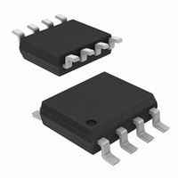
AD22151YR-REEL Analog Devices Inc, AD22151YR-REEL Datasheet - Page 4

AD22151YR-REEL
Manufacturer Part Number
AD22151YR-REEL
Description
IC MAGNETIC FIELD SNSR LIN 8SOIC
Manufacturer
Analog Devices Inc
Type
Linear - Unipolar, Bipolarr
Datasheet
1.AD22151YRZ.pdf
(8 pages)
Specifications of AD22151YR-REEL
Rohs Status
RoHS non-compliant
Sensing Range
Unlimited
Voltage - Supply
4.5 V ~ 6 V
Current - Supply
10mA
Current - Output (max)
15mA
Output Type
Analog, Ratiometric
Operating Temperature
-40°C ~ 150°C
Package / Case
8-SOIC (0.154", 3.90mm Width)
Features
-
AD22151
Figure 6. Gain Variation from 25 ∞ C vs. Temperature
(–200 ppm) Field; R1 –15 k W
Figure 5. Signal Drift over Temperature (–40 ∞ C to
+150 ∞ C) vs. Field (–200 ppm); 5 V Supply
Figure 7. Signal Drift over Temperature (–40 ∞ C to
+150 ∞ C) vs. Field (–2000 ppm); 5 V Supply
–0.05
0.025
0.020
0.015
0.010
0.005
0.020
0.20
0.045
0.040
0.035
0.030
0.025
0.015
0.010
0.005
0.25
0.15
0.10
0.05
0
–600
–40
0
–800
0
–600
–400
–400
10
–200
TEMPERATURE – C
–200
FIELD – Gauss
FIELD – Gauss
60
0
0
200
200
110
400
400
600
160
600
800
–4–
TEMPERATURE COMPENSATION
The AD22151 incorporates a “thermistor” transducer that
detects relative chip temperature within the package. This
function provides a compensation mechanism for the various
temperature dependencies of the Hall cell and magnet combina-
tions. The temperature information is accessible at Pins 1 and
2 (
sented by Figure 9. The compensation voltages are trimmed
to converge at V
the negative TC voltage via an internal resistor (see the Func-
tional Block Diagram). An external resistor connected between
Pin 3 and Pins 1 or 2 will produce a potential division of the
two complementary TC voltages to provide optimal compensa-
tion. The Pin 3 internal resistor provides a secondary TC
designed to reduce second order Hall cell temperature sensitivity.
The voltages present at Pins 1, 2, and 3 are proportional to the
supply voltage. The presence of the Pin 2 internal resistor dis-
tinguishes the effective compensation ranges of Pins 1 and 2.
(See temperature configuration in Figures 1 and 2, and typical
resistor values in Figures 10 and 11.)
Variation occurs in the operation of the gain temperature com-
pensation for two reasons. First, the die temperature within the
package is somewhat higher than the ambient temperature due
Figure 9. TC1, TC2, and TC3 with Respect to Reference
vs. Temperature
Figure 8. Gain Variation (from 25 ∞ C) vs. Temperature
(–2000 ppm Field; R1 = 12 k W )
+2900 ppm/∞C) and Pin 3 (
–0.2
–0.2
–0.4
–0.6
–0.8
–1.0
1.8
0.8
2.0
1.6
1.4
1.2
1.0
0.8
0.6
0.4
0.2
1.0
0.6
0.4
0.2
0
0
–40
150
CC
/2 at 25∞C. Pin 3 is internally connected to
112
10
TC1, TC2 VOLTS
TEMPERATURE – C
TEMPERATURE – C
74
TC3 VOLTS
60
–2900 ppm/∞C), as repre-
36
110
–2
160
–40
REV. A


