KIT34844AEPEVBE Freescale Semiconductor, KIT34844AEPEVBE Datasheet - Page 42
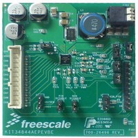
KIT34844AEPEVBE
Manufacturer Part Number
KIT34844AEPEVBE
Description
LED Lighting Development Kits IC, 10 CHANNEL LED BACKLIGHT
Manufacturer
Freescale Semiconductor
Datasheet
1.MC34844AEP.pdf
(62 pages)
Specifications of KIT34844AEPEVBE
Supply Voltage
12 V
Supply Current
2 uA
For Use With/related Products
34844A
Lead Free Status / RoHS Status
Lead free / RoHS Compliant


medium LCDs, due to some advantages over other
backlighting schemes, such as the widely used cold cathode
fluorescent lamp (CCFL). The advantages of LED
backlighting are low cost, long life, immunity to vibration, low
operational voltage, and precise control over its intensity.
requires more power than most of the other methods, and this
is a major problem if the LCD size is large enough.
optoelectronics technologies are evolving to create brighter
LEDs with lower power consumption. These new
technologies together with highly efficient power
management LED drivers are turning LEDs, a more suitable
solution for backlighting almost any size of LCD panel, with
really conservative power consumption.
LED is the one known as “Array backlighting”. This creates a
matrix of LEDs all over the LCD surface, using defraction and
diffused layers to produce an homogenous and even light at
INPUT VOLTAGE SUPPLY (VIN)
produce internal voltage regulation (VDC1, VDC3) for logic
functioning, and also as an input voltage for the boost
regulator.
INTERNAL VOLTAGE REGULATOR 1 (VDC1)
purposes. A capacitor of 2.2 μF should be connected
between this pin and ground for decoupling purposes.
INTERNAL VOLTAGE REGULATOR 2 (VDC2)
purposes. A capacitor of 2.2 μF should be connected
between this pin and ground for decoupling purposes.
INTERNAL VOLTAGE REGULATOR 3 (VDC3)
purposes. A capacitor of 2.2 μF should be connected
between this pin and ground for decoupling purposes.
BOOST COMPENSATION PIN (COMP)
Add a capacitor and a resistor in series to GND to stabilize
the system.
42
34844A
FUNCTIONAL DESCRIPTION
INTRODUCTION
LED backlighting has become very popular for small and
However, there is an important drawback of this method. It
To address the power consumption problem, solid state
One of the most common schemes for backlighting with
IC Power input supply voltage, is used internally to
This pin is for internal use only, and not to be used for other
This pin is for internal use only, and not to be used for other
This pin is for internal use only, and not to be used for other
Passive terminal used to compensate the boost converter.
FUNCTIONAL DESCRIPTION
FUNCTIONAL PIN DESCRIPTION
INTRODUCTION
the LCD surface. Each row or column is formed by a number
of LEDs in series, forcing a single current to flow through all
LEDs in each string.
system to maintain a constant current flowing through each
line, keeping a steady amount of light even with the presence
of line or load variations. They can also be use as a light
intensity control by increasing or decreasing the amount of
current flowing through each LED string.
series, a boost converter is implemented, to produce a higher
voltage from a smaller one, which is typically used by the
logical blocks to do their function.
together with 10 input channels, for driving up to 16 LEDs per
string to create a matrix of more than 160 LEDs. Together
with its 90% efficiency and I
current control, among other features, makes the 34844A a
perfect solution for backlighting small and medium size LCD
panels, on low power portable and high definition devices.
IC ENABLE (EN)
through pull-up resistors. Applying 0V to this terminal would
stop the IC from working.
INPUT/OUTPUT CLOCK SIGNAL (CK)
(master mode), or input clock signal (slave mode), to
synchronize more than one device.
MASTER/SLAVE MODE SELECTION (M/~S)
producing an output synchronization clock at the CK terminal.
Setting this pin low, puts the device in Slave mode, using the
CK pin as an input clock.
EXTERNAL PWM INPUT (PWM)
signal can be applied to modulate the LED channel directly in
absence of an I
CLOCK I
ADDRESS I
Using a current control driver, per row or column, helps the
To achieve enough voltage to drive a number of LEDs in
The 34844A implements a single channel boost converter
The active high enable terminal is internally pulled high
This terminal can be used as an output clock signal
Setting this pin High puts the device into Master mode,
This terminal is internally pulled down. An external PWM
Clock line for I
Address line for I
2
C SIGNAL (SCK)
2
C SIGNAL (SDA)
2
C interface.
2
C communication.
2
C communication.
Analog Integrated Circuit Device Data
2
C programmable or external
Freescale Semiconductor
Related parts for KIT34844AEPEVBE
Image
Part Number
Description
Manufacturer
Datasheet
Request
R

Part Number:
Description:
Manufacturer:
Freescale Semiconductor, Inc
Datasheet:
Part Number:
Description:
Manufacturer:
Freescale Semiconductor, Inc
Datasheet:
Part Number:
Description:
Manufacturer:
Freescale Semiconductor, Inc
Datasheet:
Part Number:
Description:
Manufacturer:
Freescale Semiconductor, Inc
Datasheet:
Part Number:
Description:
Manufacturer:
Freescale Semiconductor, Inc
Datasheet:
Part Number:
Description:
Manufacturer:
Freescale Semiconductor, Inc
Datasheet:
Part Number:
Description:
Manufacturer:
Freescale Semiconductor, Inc
Datasheet:
Part Number:
Description:
Manufacturer:
Freescale Semiconductor, Inc
Datasheet:
Part Number:
Description:
Manufacturer:
Freescale Semiconductor, Inc
Datasheet:
Part Number:
Description:
Manufacturer:
Freescale Semiconductor, Inc
Datasheet:
Part Number:
Description:
Manufacturer:
Freescale Semiconductor, Inc
Datasheet:
Part Number:
Description:
Manufacturer:
Freescale Semiconductor, Inc
Datasheet:
Part Number:
Description:
Manufacturer:
Freescale Semiconductor, Inc
Datasheet:
Part Number:
Description:
Manufacturer:
Freescale Semiconductor, Inc
Datasheet:
Part Number:
Description:
Manufacturer:
Freescale Semiconductor, Inc
Datasheet: