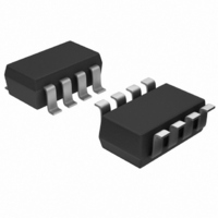
AD5273BRJZ1-REEL7 Analog Devices Inc, AD5273BRJZ1-REEL7 Datasheet - Page 20

AD5273BRJZ1-REEL7
Manufacturer Part Number
AD5273BRJZ1-REEL7
Description
IC,Digital Potentiometer,TSSOP,8PIN,PLASTIC
Manufacturer
Analog Devices Inc
Datasheet
1.AD5273BRJZ1-REEL7.pdf
(24 pages)
Specifications of AD5273BRJZ1-REEL7
Package / Case
SOT-23-8
Mounting Type
Surface Mount
Voltage - Supply
2.7 V ~ 5.5 V
Operating Temperature
-40°C ~ 105°C
Temperature Coefficient
300 ppm/°C Typical
Interface
I²C, 2-Wire Serial
Resistance In Ohms
1.00K
Number Of Circuits
1
Memory Type
Non-Volatile
Taps
64
Number Of Elements
1
# Of Taps
64
Resistance (max)
1KOhm
Power Supply Requirement
Single
Interface Type
Serial (2-Wire/I2C)
Single Supply Voltage (typ)
5V
Dual Supply Voltage (typ)
Not RequiredV
Single Supply Voltage (min)
2.7V
Single Supply Voltage (max)
5.5V
Dual Supply Voltage (min)
Not RequiredV
Dual Supply Voltage (max)
Not RequiredV
Operating Temp Range
-40C to 105C
Operating Temperature Classification
Industrial
Mounting
Surface Mount
Pin Count
8
Lead Free Status / RoHS Status
Lead free / RoHS Compliant
Lead Free Status / RoHS Status
Lead free / RoHS Compliant
Available stocks
Company
Part Number
Manufacturer
Quantity
Price
Company:
Part Number:
AD5273BRJZ1-REEL7
Manufacturer:
ADI
Quantity:
2 396
AD5273
Depending on the op amp GBP, reducing the feedback resistor
may extend the zero’s frequency far enough to overcome the
problem. A better approach is to include a compensation
capacitor, C2, to cancel the effect caused by C1. Optimum
compensation occurs when R1 × C1 = R2 × C2, but this is not
an option because of the variation of R2. As a result, users can
use the relationship described and scale C2 as if R2 were at its
maximum value. However, doing so may overcompensate by
slowing down the settling time when R2 is set to low values. To
avoid this problem, C2 should be found empirically for a given
application. In general, setting C2 in the range of a few picofarads
to no more than a few tenths of a picofarad is usually adequate
for compensation.
There is also a Terminal W capacitance connected to the output
(not shown); its effect on stability is less significant; therefore,
compensation is not necessary unless the op amp is driving a
large capacitive load.
PROGRAMMABLE LOW-PASS FILTER
In ADC applications, it is common to include an antialiasing
filter to band-limit the sampling signal. To minimize various
system redesigns, users can use two 1 kΩ AD5273s to construct
a generic second-order Sallen-Key low-pass filter. Because the
AD5273 is a single-supply device, the input must be dc offset
when an ac signal is applied to avoid clipping at ground. This is
illustrated in Figure 50. The design equations are
Users can first select some convenient values for the capacitors.
To achieve maximally flat bandwidth where Q = 0.707, let C1 be
twice the size of C2 and let R1 = R2. As a result, R1 and R2 can
be adjusted to the same setting to achieve the desired bandwidth.
Q
V
ω
V
O
O
I
=
=
=
R1C1
V
S
1
I
2
R
+
1R2C1C2
SAME SETTINGS
+
ADJUSTED TO
ω
A
Q
Figure 50. Sallen Key Low-Pass Filter
ω
R2C2
1
O
R1
O
1
S
W
2
B
+
ω
A
O
R2
2
W
B
C2
C1
C
C
U1
AD8601
+2.5V
–2.5V
V+
V–
V
O
Rev. G | Page 20 of 24
(6)
(7)
(8)
LEVEL SHIFT FOR DIFFERENT VOLTAGES
OPERATION
If the SCL and SDA signals come from a low voltage logic
controller and are below the minimum V
level-shift the signals for successful read/write communication
between the AD5273 and the controller. Figure 51 shows one of
the implementations. For example, when SDA1 is 2.5 V, M1
turns off, and SDA2 becomes 5 V. When SDA1 is 0 V, M1 turns
on, and SDA2 approaches 0 V. As a result, proper level-shifting
is established. M1 and M2 should be low threshold N-Channel
power MOSFETs, such as FDV301N.
SDA1
SCL1
RDAC CIRCUIT SIMULATION MODEL
The internal parasitic capacitances and the external capacitive
loads dominate the ac characteristics of the digital potentio-
meters. Configured as a potentiometer divider, the −3 dB
bandwidth of the AD5273 (1 kΩ resistor) measures 6 MHz at
half scale. Figure 17 to Figure 20 provide the large signal BODE
plot characteristics of the four available resistor versions: 1 kΩ,
10 kΩ, 50 kΩ, and 100 kΩ. Figure 52 shows a parasitic simula-
tion model. The code following Figure 52 provides a macro
model net list for the 1 kΩ device.
Macro Model Net List for RDAC
.PARAM D = 63, RDAC = 1E3
*
.SUBCKT DPOT (A,W,B)
*
CA A 0 25E-12
RWA A W {(1-D/63)*RDAC+60}
CW W 0 55E-12
RWB W B {D/63*RDAC+60}
CB B 0 25E-12
*
.ENDS DPOT
V
DD1
CONTROLLER
= 2.5V
2.5V
Figure 51. Level Shift for Different Voltages Operation
Figure 52. Circuit Simulation Model for RDAC = 1 kΩ
Rp
2
5pF
C
A
A
Rp
S
M1
G
1kΩ
W
C
W
D
55pF
S
M2
G
B
C
25pF
D
Rp
IH
B
level (0.7 × V
Rp
AD5273
2.7V–5.5V
V
DD2
DD
= 5V
),
SDA2
SCL2


