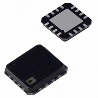
ADA4927-1YCPZ-RL Analog Devices Inc, ADA4927-1YCPZ-RL Datasheet - Page 17

ADA4927-1YCPZ-RL
Manufacturer Part Number
ADA4927-1YCPZ-RL
Description
UltraLw Distortion Crnt Fdbck ADC Driver
Manufacturer
Analog Devices Inc
Datasheet
1.ADA4927-2YCPZ-R2.pdf
(24 pages)
Specifications of ADA4927-1YCPZ-RL
Amplifier Type
Current Feedback
Number Of Circuits
1
Output Type
Differential
Slew Rate
5000 V/µs
-3db Bandwidth
2.3GHz
Current - Input Bias
500nA
Voltage - Input Offset
300µV
Current - Supply
20mA
Current - Output / Channel
65mA
Voltage - Supply, Single/dual (±)
4.5 V ~ 11 V, ±2.25 V ~ 5.5 V
Operating Temperature
-40°C ~ 105°C
Mounting Type
Surface Mount
Package / Case
16-LFCSP
Lead Free Status / RoHS Status
Lead free / RoHS Compliant
Gain Bandwidth Product
-
Lead Free Status / RoHS Status
Lead free / RoHS Compliant
APPLICATIONS INFORMATION
ANALYZING AN APPLICATION CIRCUIT
The ADA4927 uses high open-loop transimpedance and negative
current feedback to control its differential output voltage in
such a way as to minimize the differential error currents. The
differential error currents are defined as the currents that flow
in and out of the differential inputs labeled +IN and −IN (see
Figure 46). For most purposes, these currents can be assumed
to be zero. The voltage between the +IN and −IN inputs is
internally bootstrapped to 0 V; therefore, the voltages at the
amplifier inputs are equal, and external analysis can be carried
out in a similar fashion to that of voltage feedback amplifiers.
Similarly, the difference between the actual output common-
mode voltage and the voltage applied to V
to be zero. Starting from these principles, any application circuit
can be analyzed.
SETTING THE CLOSED-LOOP GAIN
Using the approach previously described, the differential gain of
the circuit in Figure 46 can be determined by
This presumes that the input resistors (R
resistors (R
Table 11. Output Noise Voltage Density Calculations for Matched Feedback Networks
Input Noise Contribution
Differential Input
Inverting Input
Noninverting Input
V
Gain Resistor, R
Gain Resistor, R
Feedback Resistor, R
Feedback Resistor, R
OCM
Input
V
V
OUT
IN
,
,
dm
dm
F
) on each side are of equal value.
=
G1
G2
R
R
G
F
F1
F2
Input Noise Term
v
i
i
v
v
v
v
v
nIN
nIN
nIN
nCM
nRG1
nRG2
nRF1
nRF2
OCM
G
) and feedback
can also be assumed
Input Noise
Voltage Density
v
i
i
v
(4kTR
(4kTR
(4kTR
(4kTR
nIN
nIN
nIN
nCM
Rev. A | Page 17 of 24
× (R
× (R
G1
G2
F1
F2
)
)
F2
F1
)
)
1/2
1/2
1/2
1/2
)
)
ESTIMATING THE OUTPUT NOISE VOLTAGE
The differential output noise of the ADA4927 can be estimated
using the noise model in Figure 47. The input-referred noise
voltage density, v
noise currents, i
ground. The output voltage due to v
v
noise currents are uncorrelated with the same mean-square value,
and each produces an output voltage that is equal to the noise
current multiplied by the associated feedback resistance. The
noise voltage density at the V
networks have the same feedback factor, as in most cases, the
output noise due to v
resistors contributes (4kTR
resistors appears directly at the output, and the noise from each
gain resistor appears at the output multiplied by R
summarizes the input noise sources, the multiplication factors,
and the output-referred noise density terms.
nIN
by the noise gain, G
Output
Multiplication Factor
G
1
1
0
R
R
1
1
F1
F2
N
/R
/R
G1
G2
V
V
nRG1
nRG2
nIN−
nIN
R
R
i
i
, is modeled as a differential input, and the
G1
G2
nIN+
nIN–
and i
nCM
Figure 47. Noise Model
N
is common mode. Each of the four
nIN+
(defined in the G
V
nIN
xx
ADA4927-1/ADA4927-2
, appear between each input and
R
R
)
OCM
1/2
F1
F2
ADA4927
. The noise from the feedback
+
pin is v
nIN
V
V
V
nRF1
OCM
nRF2
Differential Output Noise
Voltage Density Term
v
v
v
v
v
v
v
v
is obtained by multiplying
nO1
nO2
nO3
nO4
nO5
nO6
nO7
nO8
= G
= (i
= (i
= 0
= (R
= (R
= (4kTR
= (4kTR
nCM
N
nIN
nIN
N
. When the feedback
F1
F2
V
equation). The
(v
)(R
)(R
/R
/R
nOD
V
nIN
nCM
F
F1
F2
G1
G2
/R
F2
F1
)
)
)
)(4kTR
)(4kTR
)
)
1/2
1/2
G
. Table 11
G1
G2
)
)
1/2
1/2


