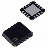
ADA4927-1YCPZ-RL Analog Devices Inc, ADA4927-1YCPZ-RL Datasheet - Page 23

ADA4927-1YCPZ-RL
Manufacturer Part Number
ADA4927-1YCPZ-RL
Description
UltraLw Distortion Crnt Fdbck ADC Driver
Manufacturer
Analog Devices Inc
Datasheet
1.ADA4927-2YCPZ-R2.pdf
(24 pages)
Specifications of ADA4927-1YCPZ-RL
Amplifier Type
Current Feedback
Number Of Circuits
1
Output Type
Differential
Slew Rate
5000 V/µs
-3db Bandwidth
2.3GHz
Current - Input Bias
500nA
Voltage - Input Offset
300µV
Current - Supply
20mA
Current - Output / Channel
65mA
Voltage - Supply, Single/dual (±)
4.5 V ~ 11 V, ±2.25 V ~ 5.5 V
Operating Temperature
-40°C ~ 105°C
Mounting Type
Surface Mount
Package / Case
16-LFCSP
Lead Free Status / RoHS Status
Lead free / RoHS Compliant
Gain Bandwidth Product
-
Lead Free Status / RoHS Status
Lead free / RoHS Compliant
HIGH PERFORMANCE ADC DRIVING
The ADA4927 is ideally suited for high gain, broadband ac-
coupled and differential-to-differential applications on a single
supply, though other applications are possible. Compared with
voltage feedback amplifiers, the current feedback architecture
provides superior distortion and bandwidth performance at
high gains. This is because the ideal current feedback amplifier
loop gain depends only on the feedback value and open-loop
transimpedance, T(s).
The circuit in Figure 58 shows a front-end connection for an
ADA4927 driving an AD9445, 14-bit, 105 MSPS ADC, with ac
coupling on the ADA4927 input and output. (The AD9445
achieves its optimum performance when driven differentially.)
The ADA4927 eliminates the need for a transformer to drive
the ADC and performs a single-ended-to-differential conversion
and buffering of the driving signal.
The ADA4927 is configured with a single 5 V supply and gain
of 10 for a single-ended input to differential output. The 158 Ω
termination resistor, in parallel with the single-ended input
impedance of approximately 73.2 Ω, provides a 50 Ω termination
for the source. The additional 38.3 Ω at the inverting input closely
matches the parallel impedance of the 50 Ω source and the
termination resistor driving the noninverting input. Because of the
high gain, a few iterations of the termination technique described
in the Terminating a Single-Ended Input section are required.
Two objectives of the design are to make R
obtain resistor values that are close to standard 1% values.
SIGNAL
GENERATOR
50Ω
Figure 58. ADA4927 Driving an AD9445 ADC with AC-Coupled Input and Output
0.1µF
158Ω
0.1µF
F
close to 500 Ω and
39.2Ω
39.2Ω
38.3Ω
0.1µF
V
OCM
+
ADA4927
511Ω
511Ω
5V
Rev. A | Page 23 of 24
0.1µF
0.1µF
24.3Ω
24.3Ω
In this example, the signal generator has a 1 V p-p symmetric,
ground-referenced bipolar output when terminated in 50 Ω.
The V
and left floating such that the internal divider sets the output
common-mode voltage nominally at midsupply. Because the
inputs are ac-coupled, no dc common-mode current flows in
the feedback loops, and a nominal dc level of midsupply is
present at the amplifier input terminals. Besides placing the
amplifier inputs at their optimum levels, the ac coupling technique
lightens the load on the amplifier and dissipates less power than
applications with dc-coupled inputs.
The output of the amplifier is ac-coupled to the ADC through a
second-order, low-pass filter with a cutoff frequency of 100 MHz.
This reduces the noise bandwidth of the amplifier and isolates
the driver outputs from the ADC inputs.
The AD9445 is configured for a 2 V p-p full-scale input by
connecting the SENSE pin to AGND, as shown in Figure 58.
30nH
30nH
OCM
VIN–
47pF
VIN+
pin of the ADA4927 is bypassed for noise reduction
AVDD2
5V (A)
BUFFER T/H
CLOCK/
TIMING
3.3V (A)
AVDD1
AGND
ADA4927-1/ADA4927-2
3.3V (D)
DRVDD
REF
ADC
SENSE
AD9445
14


