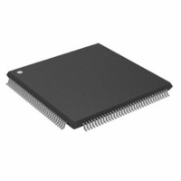
ADSP-2191MBSTZ-140 Analog Devices Inc, ADSP-2191MBSTZ-140 Datasheet - Page 24

ADSP-2191MBSTZ-140
Manufacturer Part Number
ADSP-2191MBSTZ-140
Description
IC,DSP,16-BIT,CMOS,QFP,144PIN,PLASTIC
Manufacturer
Analog Devices Inc
Series
ADSP-21xxr
Type
Fixed Pointr
Specifications of ADSP-2191MBSTZ-140
Interface
Host Interface, SPI, SSP, UART
Clock Rate
140MHz
Non-volatile Memory
External
On-chip Ram
160kB
Voltage - I/o
3.00V, 3.30V
Voltage - Core
2.50V
Operating Temperature
-40°C ~ 85°C
Mounting Type
Surface Mount
Package / Case
144-LQFP
Device Core Size
16b
Clock Freq (max)
140MHz
Mips
140
Device Input Clock Speed
140MHz
Ram Size
160KB
Operating Supply Voltage (typ)
2.5/3.3V
Operating Supply Voltage (min)
2.37/2.97V
Operating Supply Voltage (max)
2.63/3.6V
Operating Temp Range
-40C to 85C
Operating Temperature Classification
Industrial
Mounting
Surface Mount
Pin Count
144
Package Type
LQFP
Lead Free Status / RoHS Status
Lead free / RoHS Compliant
Lead Free Status / RoHS Status
Lead free / RoHS Compliant
Other names
ADSP-2191MBSTZ140
Available stocks
Company
Part Number
Manufacturer
Quantity
Price
Company:
Part Number:
ADSP-2191MBSTZ-140
Manufacturer:
MAXIM
Quantity:
101
Company:
Part Number:
ADSP-2191MBSTZ-140
Manufacturer:
Analog Devices Inc
Quantity:
10 000
ADSP-2191M
External Port Bus Request and Grant Cycle Timing
Table 14
bus grant operations.
Table 14. External Port Bus Request and Grant Cycle Timing
1
2
t
These are timing parameters that are based on worst-case operating conditions.
Parameter
Switching Characteristics
t
t
t
t
t
t
Timing Requirements
t
t
HCLK
SD
SE
DBG
EBG
DBH
EBH
BS
BH
is the peripheral clock period.
and
CLKOUT
MS3--0
A21–0
IOMS
BMS
BGH
1, 2
Figure 13
WR
BR
RD
BG
CLKOUT High to xMS, Address, and RD/WR Disable
CLKOUT Low to xMS, Address, and RD/WR Enable
CLKOUT High to BG Asserted Setup
CLKOUT High to BG Deasserted Hold Time
CLKOUT High to BGH Asserted Setup
CLKOUT High to BGH Deasserted Hold Time
BR Asserted to CLKOUT High Setup
CLKOUT High to BR Deasserted Hold Time
describe external port bus request and
t
BS
Figure 13. External Port Bus Request and Grant Cycle Timing
t
BH
–24–
t
t
t
t
t
SD
SD
SD
DBG
DBH
Min
0
0
0
0
0
4.6
0
Max
0.5t
4
4
4
4
4
t
t
EBG
HCLK
EBH
+1
t
t
t
SE
SE
SE
REV. A
Unit
ns
ns
ns
ns
ns
ns
ns
ns


