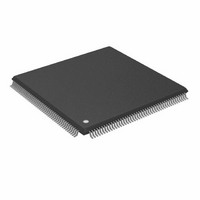
ADSP-21992BSTZ Analog Devices Inc, ADSP-21992BSTZ Datasheet - Page 6

ADSP-21992BSTZ
Manufacturer Part Number
ADSP-21992BSTZ
Description
Mixed Signal DSP W/32K DM RAM& 16K PMRAM
Manufacturer
Analog Devices Inc
Series
ADSP-21xxr
Type
Fixed Pointr
Datasheet
1.ADSP-21992BSTZ.pdf
(60 pages)
Specifications of ADSP-21992BSTZ
Interface
SPI, SSP
Clock Rate
160MHz
Non-volatile Memory
External
On-chip Ram
128kB
Voltage - I/o
3.30V
Voltage - Core
2.50V
Operating Temperature
-40°C ~ 85°C
Mounting Type
Surface Mount
Package / Case
176-LQFP
Lead Free Status / RoHS Status
Lead free / RoHS Compliant
Available stocks
Company
Part Number
Manufacturer
Quantity
Price
Company:
Part Number:
ADSP-21992BSTZ
Manufacturer:
AD
Quantity:
430
Company:
Part Number:
ADSP-21992BSTZ
Manufacturer:
Analog Devices Inc
Quantity:
10 000
ADSP-21992
The ADSP-21992 has 4K words of on-chip ROM that holds
boot routines. The DSP starts executing instructions from the
on-chip boot ROM, which starts the boot process.
information, see Booting Modes on Page 14.
ROM is located on Page 255 in the DSP memory space map,
starting at address 0xFF0000.
External (Off-Chip) Memory
Each of the off-chip memory spaces of the ADSP-21992 has a
separate control register, so applications can configure unique
access parameters for each space. The access parameters include
read and write wait counts, wait state completion mode, I/O
clock divide ratio, write hold time extension, strobe polarity,
and data bus width. The core clock and peripheral clock ratios
influence the external memory access strobe widths.
information, see Clock Signals on Page 13.
ory spaces are:
All of these off-chip memory spaces are accessible through the
external port, which can be configured for 8-bit or 16-bit
data widths.
External Memory Space
External memory space consists of four memory banks. These
banks can contain a configurable number of 64K word pages. At
reset, the page boundaries for external memory have Bank0
containing pages 1 to 63, Bank1 containing pages 64 to 127,
Bank2 containing pages 128 to 191, and Bank3 containing pages
192 to 254. The MS3-0 memory bank pins select Banks 3-0,
respectively. Both the ADSP-2199x core and DMA capable
peripherals can access the DSP external memory space.
All accesses to external memory are managed by the external
memory interface unit (EMI).
I/O Memory Space
The ADSP-21992 supports an additional external memory
called I/O memory space. The I/O space consists of 256 pages,
each containing 1024 addresses. This space is designed to sup-
port simple connections to peripherals (such as data converters
and external registers) or to bus interface ASIC data registers.
The first 32K addresses (I/O pages 0 to 31) are reserved for on-
chip peripherals. The upper 224K addresses (I/O pages 32 to
• External memory space (MS3–0 pins)
• I/O memory space (IOMS pin)
• Boot memory space (BMS pin)
register to supply the most significant eight address bits.
Before a cross page jump or call, the program must set the
program sequencer IJPG register to the appropriate mem-
ory page.
The off-chip mem-
The on-chip boot
For more
Rev. A | Page 6 of 60 | August 2007
For more
255) are available for external peripheral devices. External I/O
pages have their own select pin (IOMS). The DSP instruction set
provides instructions for accessing I/O space.
Boot Memory Space
Boot memory space consists of one off-chip bank with 254
pages. The BMS memory bank pin selects boot memory space.
Both the ADSP-2199x core and DMA capable peripherals can
access the DSP off-chip boot memory space. After reset, the
DSP always starts executing instructions from the on-chip
boot ROM.
BUS REQUEST AND BUS GRANT
The ADSP-21992 can relinquish control of the data and address
buses to an external device. When the external device requires
access to the bus, it asserts the bus request (BR) signal. The (BR)
signal is arbitrated with core and peripheral requests. External
bus requests have the lowest priority. If no other internal
request is pending, the external bus request will be granted. Due
to synchronizer and arbitration delays, bus grants will be pro-
vided with a minimum of three peripheral clock delays. The
ADSP-21992 will respond to the bus grant by:
• Three-stating the data and address buses and the MS3–0,
• Asserting the bus grant (BG) signal.
BMS, IOMS, RD, and WR output drivers.
0x00::0x000
0x1F::0x3FF
0x20::0x000
0xFF::0x3FF
0x01 0000
0xFE 0000
Figure 5. Boot Memory Map
Figure 4. I/O Memory Map
PERIPHERALS
PERIPHERALS
BOOT MEMORY
OFF-CHIP
ON-CHIP
16-BITS
16-BITS
OFF-CHIP
16-BITS
PAGES 0 TO 31
1024 WORDS/PAGE
2 PERIPHERALS/PAGE
PAGES 32 TO 255
1024 WORDS/PAGE
PAGES 1 TO 254
64K WORDS/PAGE


