ADV212BBCZ-115 Analog Devices Inc, ADV212BBCZ-115 Datasheet - Page 20
ADV212BBCZ-115
Manufacturer Part Number
ADV212BBCZ-115
Description
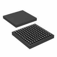
IC,Compression/Decompression Processor,BGA,121PIN,PLASTIC
Manufacturer
Analog Devices Inc
Series
Wavescale®r
Type
JPEG2000 Video Codecr
Datasheet
1.ADV212BBCZRL-115.pdf
(44 pages)
Specifications of ADV212BBCZ-115
Resolution (bits)
16 b
Sigma Delta
No
Voltage - Supply, Analog
1.5V, 3.3V
Voltage - Supply, Digital
1.5V, 3.3V
Operating Temperature
-40°C ~ 85°C
Mounting Type
Surface Mount
Package / Case
121-CSPBGA
Lead Free Status / RoHS Status
Lead free / RoHS Compliant
For Use With
ADV212-HD-EB - BOARD EVALUATION FOR ADV212-HD
Lead Free Status / Rohs Status
Compliant
Available stocks
Company
Part Number
Manufacturer
Quantity
Price
Company:

Part Number:
ADV212BBCZ-115
Manufacturer:
INTEGRAL
Quantity:
1 430
Company:
Part Number:
ADV212BBCZ-115
Manufacturer:
ADI
Quantity:
672
Company:
Part Number:
ADV212BBCZ-115
Manufacturer:
Analog Devices Inc
Quantity:
10 000


ADV212
PIN CONFIGURATIONS AND FUNCTION DESCRIPTIONS
Table 16. Pin Function Descriptions
Pin No.
119
117
37 to 34,
27 to 25,
16, 15, 24,
14 to 12,
2, 6, 5
88, 107,
87, 97
96
95
86
121-Ball Package
Location
L9
L7
D4 to D1,
C5 to C3,
B5, B4, C2,
B3 to B1,
A2, A6, A5
H11, K8,
H10, J9
J8
J7
H9
Figure 30.121-Ball Pin Configuration
11
10
9
BOTTOM VIEW
(Not to Scale)
8 7 6
Pin No.
132
131
64, 49 to
51, 37 to
39, 25 to
27, 13 to
15, 2 to 4
108 to 106,
96
95
94
84
5 4
144-Ball Package
3 2 1
A
B
C
D
E
F
G
H
J
K
L
Location
L12
L11
F4, E1 to E3,
D1 to D3,
C1 to C3,
B1 to B3,
A2 to A4
J12 to J10,
H12
H11
H10
G12
Mnemonic
MCLK
RESET
HDATA[15:0]
ADDR[3:0]
CS
WE
RDFB
RD
WEFB
Rev. B | Page 20 of 44
1
1
2
3
Pins
Used
1
1
16
4
1
1
1
Type
I
I
I/O
I
I
I
I
Figure 31. 144-Ball Pin Configuration
Description
System Input Clock. See the PLL Registers
section.
Reset. Causes the ADV212 to immediately reset.
CS, RD, WE, DACK0, DACK1, DREQ0, and DREQ1
must be held high when a RESET is applied.
Host Data Bus. With HDATA[23:16],
HDATA[27:24], and HDATA[31:28], these pins
make up the 32-bit wide host data bus. The
async host interface is interfaced together
with ADDR[3:0], CS, WE, RD, and ACK.
Unused HDATA pins should be pulled down
via a 10 kΩ resistor.
Address Bus for the Host Interface.
Chip Select. This signal is used to qualify
addressed read and write access to the
ADV212 using the host interface.
Write Enable Used with the Host Interface.
Read Enable When Fly-By DMA Is Enabled.
Simultaneous assertion of WE and DACK low
activates the HDATA bus, even if the DMA
channels are disabled.
Read Enable Used with the Host Interface.
Write Enable When Fly-By DMA Is Enabled.
Simultaneous assertion of RD and DACK low
activates the HDATA bus, even if the DMA
channels are disabled.
12
11
10
BOTTOM VIEW
9
(Not to Scale)
8
7
6
5
4
3
2
1
B
C
F
G
J
K
A
D
E
H
L
M
Related parts for ADV212BBCZ-115
Image
Part Number
Description
Manufacturer
Datasheet
Request
R

Part Number:
Description:
BOARD EVALUATION FOR ADV212-HD
Manufacturer:
Analog Devices Inc
Datasheet:

Part Number:
Description:
BOARD EVAL FOR ADV212 CODEC
Manufacturer:
Analog Devices Inc
Datasheet:

Part Number:
Description:
JPEG 2000 Video Codec
Manufacturer:
AD [Analog Devices]
Datasheet:

Part Number:
Description:
±1.7g Dual-Axis IMEMS Accelerometer Evaluation Board
Manufacturer:
Analog Devices Inc
Datasheet:
Part Number:
Description:
Inertial Sensor Evaluation System
Manufacturer:
Analog Devices Inc
Datasheet:
Part Number:
Description:
Manufacturer:
Analog Devices Inc
Datasheet:
Part Number:
Description:
Manufacturer:
Analog Devices Inc
Datasheet:
Part Number:
Description:
Manufacturer:
Analog Devices Inc
Datasheet:
Part Number:
Description:
Manufacturer:
Analog Devices Inc
Datasheet:
Part Number:
Description:
Manufacturer:
Analog Devices Inc
Datasheet:
Part Number:
Description:
Manufacturer:
Analog Devices Inc
Datasheet:
Part Number:
Description:
Manufacturer:
Analog Devices Inc
Datasheet:
Part Number:
Description:
Manufacturer:
Analog Devices Inc
Datasheet: