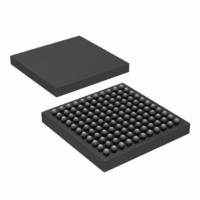
ADV212BBCZ-115 Analog Devices Inc, ADV212BBCZ-115 Datasheet - Page 21

ADV212BBCZ-115
Manufacturer Part Number
ADV212BBCZ-115
Description
IC,Compression/Decompression Processor,BGA,121PIN,PLASTIC
Manufacturer
Analog Devices Inc
Series
Wavescale®r
Type
JPEG2000 Video Codecr
Datasheet
1.ADV212BBCZRL-115.pdf
(44 pages)
Specifications of ADV212BBCZ-115
Resolution (bits)
16 b
Sigma Delta
No
Voltage - Supply, Analog
1.5V, 3.3V
Voltage - Supply, Digital
1.5V, 3.3V
Operating Temperature
-40°C ~ 85°C
Mounting Type
Surface Mount
Package / Case
121-CSPBGA
Lead Free Status / RoHS Status
Lead free / RoHS Compliant
For Use With
ADV212-HD-EB - BOARD EVALUATION FOR ADV212-HD
Lead Free Status / Rohs Status
Compliant
Available stocks
Company
Part Number
Manufacturer
Quantity
Price
Company:
Part Number:
ADV212BBCZ-115
Manufacturer:
INTEGRAL
Quantity:
1 430
Company:
Part Number:
ADV212BBCZ-115
Manufacturer:
ADI
Quantity:
672
Company:
Part Number:
ADV212BBCZ-115
Manufacturer:
Analog Devices Inc
Quantity:
10 000
Pin No.
85
76
63
64
121-Ball Package
Location
H8
G10
F8
F9
Pin No.
83
82
72
71
144-Ball Package
Location
G11
G10
F12
F11
Mnemonic
ACK
IRQ
DREQ0
FSRQ0
VALID
CFG1
DACK0
HOLD
FCS0
Rev. B | Page 21 of 44
Pins
Used
1
1
1
1
Type
O
O
O
O
O
I
I
I
I
Description
Acknowledge. Used for direct register accesses.
This signal indicates that the last register access
was successful. Due to synchronization issues,
control and status register accesses may incur an
additional delay; therefore, the host software
should wait for acknowledgment from the
ADV212 before attempting another register
access.
Accesses to the FIFOs (external DMA modes),
on the other hand, are guaranteed to occur
immediately, provided that space is available;
therefore, the host software does not need to
wait for ACK before attempting another register
access, provided that the timing constraints
are observed.
If ACK is shared with more than one device, ACK
should be connected to a pull-up resistor (10 k Ω)
and the PLL_HI register, Bit 4, must be set to 1.
Interrupt. This pin indicates that the ADV212
requires the attention of the host processor.
This pin can be programmed to indicate the
status of the internal interrupt conditions
within the ADV212. The interrupt sources are
enabled via the bits in the EIRQIE register.
Data Request for External DMA Interface.
Indicates that the ADV212 is ready to
send/receive data to/from the FIFO assigned
to DMA Channel 0.
FIFO Service Request. Used in DCS-DMA
mode. Service request from the FIFO assigned
to Channel 0 (asynchronous mode).
Valid Indication for JDATA Input/Output Stream.
Polarity of this pin is programmable in the
EDMOD0 register. VALID is always an output.
Boot Mode Configuration. This pin is read on
reset to determine the boot configuration of
the on-board processor. The pin should be
tied to IOVDD through a 10 kΩ resistor.
Data Acknowledge for External DMA Interface.
Signal from the host CPU, which indicates that
the data transfer request (DREQ0) has been
acknowledged and that the data transfer can
proceed. This pin must be held high at all
times if the DMA interface is not used, even if
the DMA channels are disabled.
External Hold Indication for JDATA Input/Output
Stream. Polarity is programmable in the
EDMOD0 register. This pin is always an input.
FIFO Chip Select. Used in DCS-DMA mode.
Chip select for the FIFO assigned to Channel 0
(asynchronous mode).
ADV212


