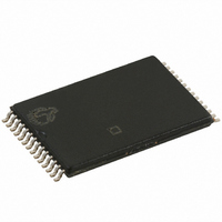
CY7C199D-10ZXIT Cypress Semiconductor Corp, CY7C199D-10ZXIT Datasheet - Page 8

CY7C199D-10ZXIT
Manufacturer Part Number
CY7C199D-10ZXIT
Description
CY7C199D-10ZXIT
Manufacturer
Cypress Semiconductor Corp
Datasheet
1.CY7C199D-10VXI.pdf
(15 pages)
Specifications of CY7C199D-10ZXIT
Format - Memory
RAM
Memory Type
SRAM - Asynchronous
Memory Size
256K (32K x 8)
Speed
10ns
Interface
Parallel
Voltage - Supply
4.5 V ~ 5.5 V
Operating Temperature
-40°C ~ 85°C
Package / Case
28-TSOP I
Lead Free Status / RoHS Status
Lead free / RoHS Compliant
Other names
428-2014-2
Available stocks
Company
Part Number
Manufacturer
Quantity
Price
Part Number:
CY7C199D-10ZXIT
Manufacturer:
CYPRESS/赛普拉斯
Quantity:
20 000
Notes
Switching Waveforms
Document Number: 38-05471 Rev. *H
16. The internal write time of the memory is defined by the overlap of CE LOW and WE LOW. Both signals must be LOW to initiate a write and either signal can terminate a
17. The minimum write cycle time for Write Cycle No. 3 (WE controlled, OE LOW) is the sum of t
18. Data I/O is high impedance if OE = V
19. If CE goes HIGH simultaneously with WE HIGH, the output remains in a high-impedance state.
20. During this period the I/Os are in the output state and input signals should not be applied.
ADDRESS
ADDRESS
DATA I/O
DATA IO
write by going HIGH. The data input setup and hold timing should be referenced to the rising edge of the signal that terminates the write.
WE
WE
CE
CE
NOTE
t
SA
20
IH
Figure 6. Write Cycle No. 3 WE Controlled, OE LOW
(continued)
.
t
Figure 5. Write Cycle No. 1: CE Controlled
HZWE
t
SA
t
t
AW
AW
t
t
WC
WC
DATA
DATA
t
SCE
HZWE
t
t
SD
SD
IN
IN
and t
VALID
VALID
SD
.
[16, 18, 19]
[17, 19]
t
HD
t
t
HA
LZWE
t
HA
t
HD
CY7C199D
Page 8 of 15
[+] Feedback


