EVAL-ADF7021-NDBZ5 Analog Devices Inc, EVAL-ADF7021-NDBZ5 Datasheet - Page 26
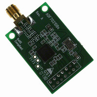
EVAL-ADF7021-NDBZ5
Manufacturer Part Number
EVAL-ADF7021-NDBZ5
Description
Matching Unpopulated
Manufacturer
Analog Devices Inc
Type
Transceiver, FSKr
Datasheet
1.ADF7021-NBCPZ-RL.pdf
(64 pages)
Specifications of EVAL-ADF7021-NDBZ5
Frequency
80MHz ~ 650MHz
Lead Free Status / RoHS Status
Lead free / RoHS Compliant
For Use With/related Products
ADF7021-N
Lead Free Status / Rohs Status
Supplier Unconfirmed


ADF7021-N
TRANSMITTER
RF OUTPUT STAGE
The power amplifier (PA) of the ADF7021-N is based on a
single-ended, controlled current, open-drain amplifier that has
been designed to deliver up to 13 dBm into a 50 Ω load at a
maximum frequency of 950 MHz.
The PA output current and consequently, the output power, are
programmable over a wide range. The PA configuration is shown
in Figure 39. The output power is set using R2_DB[13:18].
The PA is equipped with overvoltage protection, which makes it
robust in severe mismatch conditions. Depending on the appli-
cation, users can design a matching network for the PA to exhibit
optimum efficiency at the desired radiated output power level
for a wide range of antennas, such as loop or monopole antennas.
See the LNA/PA Matching section for more information.
PA Ramping
When the PA is switched on or off quickly, its changing input
impedance momentarily disturbs the VCO output frequency.
This process is called VCO pulling, and it manifests as spectral
splatter or spurs in the output spectrum around the desired carrier
frequency. Some radio emissions regulations place limits on
these PA transient-induced spurs (for example, the ETSI EN 300 220
regulations). By gradually ramping the PA on and off, PA transient
spurs are minimized.
The ADF7021-N has built-in PA ramping configurability. As
Figure 40 illustrates, there are eight ramp rate settings, defined
as a certain number of PA setting codes per one data bit period.
The PA steps through each of its 64 code levels but at different
speeds for each setting. The ramp rate is set by configuring
R2_DB[8:10].
If the PA is enabled/disabled by the PA_ENABLE bit (R2_DB7),
it ramps up and down. If it is enabled/disabled by the Tx/Rx bit
(R0_DB27), it ramps up and turns hard off.
RFGND
RFOUT
FROM VCO
+
Figure 39. PA Configuration
R2_DB(11:12)
IDAC
2
R2_DB7
R0_DB27
6
R2_DB(13:18)
Rev. 0 | Page 26 of 64
PA Bias Currents
The PA_BIAS bits (R2_DB[11:12]) facilitate an adjustment of
the PA bias current to further extend the output power control
range, if necessary. If this feature is not required, the default
value of 9 μA is recommended. If output power of greater than
10 dBm is required, a PA bias setting of 11 μA is recommended.
The output stage is powered down by resetting R2_DB7.
MODULATION SCHEMES
The ADF7021-N supports 2FSK, 3FSK, and 4FSK modulation.
The implementation of these modulation schemes is shown in
Figure 41.
RAISED COSINE
GAUSSIAN
FILTERING
(256 CODES PER BIT)
(128 CODES PER BIT)
(64 CODES PER BIT)
(32 CODES PER BIT)
(16 CODES PER BIT)
(8 CODES PER BIT)
(4 CODES PER BIT)
OR
REF
Tx_FREQUENCY_
DEVIATION
PA RAMP 0
(NO RAMP)
PA RAMP 1
PA RAMP 2
PA RAMP 3
PA RAMP 4
PA RAMP 5
PA RAMP 6
PA RAMP 7
DATA BITS
Figure 41. Transmit Modulation Implementation
FRACTIONAL_N
CHARGE
PUMP
PFD/
Figure 40. PA Ramping Settings
MUX
3FSK
4FSK
2FSK
Σ-Δ MODULATOR
LOOP FILTER
THIRD-ORDER
1
2
BIT SYMBOL
1 – D
SHAPING
MAPPER
3
4FSK
2
4
PR
...
INTEGER_N
VCO
8
÷N
CODER
...
PRE-
÷2
16
PA STAGE
TO
TxDATA
Related parts for EVAL-ADF7021-NDBZ5
Image
Part Number
Description
Manufacturer
Datasheet
Request
R

Part Number:
Description:
±1.7g Dual-Axis IMEMS Accelerometer Evaluation Board
Manufacturer:
Analog Devices Inc
Datasheet:

Part Number:
Description:
Inertial Sensor Evaluation System
Manufacturer:
Analog Devices Inc
Datasheet:
Part Number:
Description:
Manufacturer:
Analog Devices Inc
Datasheet:
Part Number:
Description:
Manufacturer:
Analog Devices Inc
Datasheet:
Part Number:
Description:
Manufacturer:
Analog Devices Inc
Datasheet:
Part Number:
Description:
Manufacturer:
Analog Devices Inc
Datasheet:
Part Number:
Description:
Manufacturer:
Analog Devices Inc
Datasheet:
Part Number:
Description:
Manufacturer:
Analog Devices Inc
Datasheet:
Part Number:
Description:
Manufacturer:
Analog Devices Inc
Datasheet:
Part Number:
Description:
Manufacturer:
Analog Devices Inc
Datasheet:
Part Number:
Description:
Manufacturer:
Analog Devices Inc
Datasheet:
Part Number:
Description:
Manufacturer:
Analog Devices Inc
Datasheet:
Part Number:
Description:
Manufacturer:
Analog Devices Inc
Datasheet: