EVAL-ADF7021-NDBZ5 Analog Devices Inc, EVAL-ADF7021-NDBZ5 Datasheet - Page 48
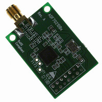
EVAL-ADF7021-NDBZ5
Manufacturer Part Number
EVAL-ADF7021-NDBZ5
Description
Matching Unpopulated
Manufacturer
Analog Devices Inc
Type
Transceiver, FSKr
Datasheet
1.ADF7021-NBCPZ-RL.pdf
(64 pages)
Specifications of EVAL-ADF7021-NDBZ5
Frequency
80MHz ~ 650MHz
Lead Free Status / RoHS Status
Lead free / RoHS Compliant
For Use With/related Products
ADF7021-N
Lead Free Status / Rohs Status
Supplier Unconfirmed


ADF7021-N
INTERFACING TO A MICROCONTROLLER/DSP
Standard Transmit/Receive Data Interface
The standard transmit/receive signal and configuration interface
to a microcontroller is shown in Figure 59. In transmit mode,
the ADF7021-N provides the data clock on the TxRxCLK pin,
and the TxRxDATA pin is used as the data input. The transmit
data is clocked into the ADF7021-N on the rising edge of
TxRxCLK.
In receive mode, the ADF7021-N provides the synchronized
data clock on the TxRxCLK pin. The receive data is available on
the TxRxDATA pin. The rising edge of TxRxCLK should be
used to clock the receive data into the microcontroller. Refer to
Figure 4 and Figure 5 for the relevant timing diagrams.
In 4FSK transmit mode, the MSB of the transmit symbol is
clocked into the ADF7021-N on the first rising edge of the data
clock from the TxRxCLK pin. In 4FSK receive mode, the MSB
of the first payload symbol is clocked out on the first negative
edge of the data clock after the SWD and should be clocked into
the microcontroller on the following rising edge. Refer to Figure 6
and Figure 7 for the relevant timing diagrams.
UART Mode
In UART mode, the TxRxCLK pin is configured to input transmit
data in transmit mode. In receive mode, the receive data is available
on the TxRxDATA pin, thus providing an asynchronous data
interface. The UART mode can only be used with oversampled
2FSK. Figure 60 shows a possible interface to a microcontroller
using the UART mode of the ADF7021-N. To enable this UART
interface mode, set R0_DB28 high. Figure 8 and Figure 9 show
the relevant timing diagrams for UART mode.
ADuC84x
GPIO
MICROCONTROLLER
Figure 59. ADuC84x to ADF7021-N Connection Diagram
P3.2/INT0
SCLOCK
UART
MISO
MOSI
P3.7
P2.4
P2.5
P2.6
P2.7
SS
Asynchronous Microcontroller Interface
GPIO
Figure 60. ADF7021-N (UART Mode) to
RxDATA
TxDATA
TxRxCLK
TxRxDATA
CE
SWD
SREAD
SLE
SDATA
SCLK
ADF7021-N
TxRxDATA
TxRxCLK
CE
SWD
SREAD
SLE
SDATA
SCLK
ADF7021-N
Rev. 0 | Page 48 of 64
SPI Mode
In SPI mode, the TxRxCLK pin is configured to input transmit
data in transmit mode. In receive mode, the receive data is available
on the TxRxDATA pin. The data clock in both transmit and receive
modes is available on the CLKOUT pin. In transmit mode, data is
clocked into the ADF7021-N on the positive edge of CLKOUT. In
receive mode, the TxRxDATA data pin should be sampled by
the microcontroller on the positive edge of the CLKOUT.
To enable SPI interface mode, set R0_DB28 high and set
R15_DB[17:19] to 0x7. Figure 8 and Figure 9 show the relevant
timing diagrams for SPI mode, while Figure 61 shows the
recommended interface to a microcontroller using the SPI
mode of the ADF7021-N.
ADSP-BF533 interface
The suggested method of interfacing to the Blackfin® ADSP-
BF533 is given in Figure 62.
ADSP-BF533
Figure 61. ADF7021-N (SPI Mode) to Microcontroller Interface
MICROCONTROLLER
Figure 62. ADSP-BF533 to ADF7021-N Connection Diagram
RSCLK1
DR1PRI
DT1PRI
MOSI
MISO
RFS1
SCK
PF5
PF6
SPI
GPIO
SCLK
MISO
MOSI
TxRxCLK
TxRxDATA
CLKOUT
CE
SWD
SREAD
SLE
SDATA
SCLK
ADF7021-N
SCLK
SDATA
SREAD
SLE
TxRxCLK
TxRxDATA
SWD
CE
ADF7021-N
Related parts for EVAL-ADF7021-NDBZ5
Image
Part Number
Description
Manufacturer
Datasheet
Request
R

Part Number:
Description:
±1.7g Dual-Axis IMEMS Accelerometer Evaluation Board
Manufacturer:
Analog Devices Inc
Datasheet:

Part Number:
Description:
Inertial Sensor Evaluation System
Manufacturer:
Analog Devices Inc
Datasheet:
Part Number:
Description:
Manufacturer:
Analog Devices Inc
Datasheet:
Part Number:
Description:
Manufacturer:
Analog Devices Inc
Datasheet:
Part Number:
Description:
Manufacturer:
Analog Devices Inc
Datasheet:
Part Number:
Description:
Manufacturer:
Analog Devices Inc
Datasheet:
Part Number:
Description:
Manufacturer:
Analog Devices Inc
Datasheet:
Part Number:
Description:
Manufacturer:
Analog Devices Inc
Datasheet:
Part Number:
Description:
Manufacturer:
Analog Devices Inc
Datasheet:
Part Number:
Description:
Manufacturer:
Analog Devices Inc
Datasheet:
Part Number:
Description:
Manufacturer:
Analog Devices Inc
Datasheet:
Part Number:
Description:
Manufacturer:
Analog Devices Inc
Datasheet:
Part Number:
Description:
Manufacturer:
Analog Devices Inc
Datasheet: