EVAL-ADF7021-NDBZ5 Analog Devices Inc, EVAL-ADF7021-NDBZ5 Datasheet - Page 40
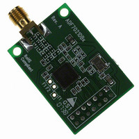
EVAL-ADF7021-NDBZ5
Manufacturer Part Number
EVAL-ADF7021-NDBZ5
Description
Matching Unpopulated
Manufacturer
Analog Devices Inc
Type
Transceiver, FSKr
Datasheet
1.ADF7021-NBCPZ-RL.pdf
(64 pages)
Specifications of EVAL-ADF7021-NDBZ5
Frequency
80MHz ~ 650MHz
Lead Free Status / RoHS Status
Lead free / RoHS Compliant
For Use With/related Products
ADF7021-N
Lead Free Status / Rohs Status
Supplier Unconfirmed


ADF7021-N
External Rx/Tx Switch
Figure 51 shows a configuration using an external Rx/Tx switch.
This configuration allows an independent optimization of the
matching and filter network in the transmit and receive path.
Therefore, it is more flexible and less difficult to design than the
configuration using the internal Rx/Tx switch. The PA is biased
through Inductor L1, while C1 blocks dc current. Together, L1
and C1 form the matching network that transforms the source
impedance into the optimum PA load impedance, Z
Z
output power, the frequency range, the supply voltage range,
and the temperature range. Selecting an appropriate Z
helps to minimize the Tx current consumption in the application.
Application Note AN-764 and Application Note AN-859 contain a
number of Z
certain conditions, however, it is recommended to obtain a suitable
Z
Due to the differential LNA input, the LNA matching network
must be designed to provide both a single-ended-to-differential
conversion and a complex, conjugate impedance match. The
network with the lowest component count that can satisfy these
requirements is the configuration shown in Figure 51, consisting
of two capacitors and one inductor.
ANTENNA
Rx/Tx – SELECT
OPT
OPT
_PA value by means of a load-pull measurement.
_PA depends on various factors, such as the required
ADG919
Figure 51. ADF7021-N with External Rx/Tx Switch
OPT
_PA values for representative conditions. Under
OPTIONAL
OPTIONAL
(SAW)
BPF
LPF
C
C
C1
B
A
V
BAT
Z
Z
Z
L
OPT
IN
IN
A
L1
_RFIN
_RFIN
_PA
ADF7021-N
PA_OUT
RFIN
RFINB
OPT
LNA
OPT
_PA.
PA
_PA
Rev. 0 | Page 40 of 64
Depending on the antenna configuration, the user may need a
harmonic filter at the PA output to satisfy the spurious emission
requirement of the applicable government regulations. The
harmonic filter can be implemented in various ways, for example, a
discrete LC pi or T-stage filter. The immunity of the ADF7021-N
to strong out-of-band interference can be improved by adding a
band-pass filter in the Rx path. Alternatively, the ADF7021-N
blocking performance can be improved by selecting one of the
enhanced linearity modes, as described in Table 15.
IMAGE REJECTION CALIBRATION
The image channel in the ADF7021-N is 200 kHz below the
desired signal. The polyphase filter rejects this image with an
asymmetric frequency response. The image rejection performance
of the receiver is dependent on how well matched the I and Q
signals are in amplitude and how well matched the quadrature
is between them (that is, how close to 90° apart they are). The
uncalibrated image rejection performance is approximately
29 dB (at 450 MHz). However, it is possible to improve on this
performance by as much as 20 dB by finding the optimum I/Q
gain and phase adjust settings.
Calibration Using Internal RF Source
With the LNA powered off, an on-chip generated, low level RF
tone is applied to the mixer inputs. The LO is adjusted to make
the tone fall at the image frequency where it is attenuated by the
image rejection of the IF filter. The power level of this tone is then
measured using the RSSI readback. The I/Q gain and phase adjust
DACs (R5_DB[20:31]) are adjusted and the RSSI is remeasured.
This process is repeated until the optimum values for the gain
and phase adjust are found that provide the lowest RSSI readback
level, thereby maximizing the image rejection performance of
the receiver.
Related parts for EVAL-ADF7021-NDBZ5
Image
Part Number
Description
Manufacturer
Datasheet
Request
R

Part Number:
Description:
±1.7g Dual-Axis IMEMS Accelerometer Evaluation Board
Manufacturer:
Analog Devices Inc
Datasheet:

Part Number:
Description:
Inertial Sensor Evaluation System
Manufacturer:
Analog Devices Inc
Datasheet:
Part Number:
Description:
Manufacturer:
Analog Devices Inc
Datasheet:
Part Number:
Description:
Manufacturer:
Analog Devices Inc
Datasheet:
Part Number:
Description:
Manufacturer:
Analog Devices Inc
Datasheet:
Part Number:
Description:
Manufacturer:
Analog Devices Inc
Datasheet:
Part Number:
Description:
Manufacturer:
Analog Devices Inc
Datasheet:
Part Number:
Description:
Manufacturer:
Analog Devices Inc
Datasheet:
Part Number:
Description:
Manufacturer:
Analog Devices Inc
Datasheet:
Part Number:
Description:
Manufacturer:
Analog Devices Inc
Datasheet:
Part Number:
Description:
Manufacturer:
Analog Devices Inc
Datasheet:
Part Number:
Description:
Manufacturer:
Analog Devices Inc
Datasheet:
Part Number:
Description:
Manufacturer:
Analog Devices Inc
Datasheet: