MT9T031C12STC Aptina LLC, MT9T031C12STC Datasheet - Page 9
MT9T031C12STC
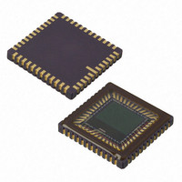
Manufacturer Part Number
MT9T031C12STC
Description
IC SENSOR IMAGE COLOR 48CLCC
Manufacturer
Aptina LLC
Series
Micron®DigitalClarity®r
Type
CMOS Imagingr
Datasheets
1.MT9T031C12STCH_ES.pdf
(12 pages)
2.MT9T031C12STCH_ES.pdf
(2 pages)
3.MT9T031C12STC.pdf
(2 pages)
4.MT9T031C12STC.pdf
(46 pages)
Specifications of MT9T031C12STC
Pixel Size
3.2µm x 3.2µm
Active Pixel Array
2048H x 1536V
Frames Per Second
12 ~ 93
Voltage - Supply
3 V ~ 3.6 V
Package / Case
48-CLCC
Brief Features
Superior Low Light Performance, Programmable Controls, Low Dark Current, High Frame Rate
Supply Voltage Range
3V To 3.6V
Operating Temperature Range
0°C To +60°C
Ic Function
Digital Image Sensor
Lead Free Status / RoHS Status
Lead free / RoHS Compliant
For Use With
557-1450 - KIT HEAD BOARD FOR MT9T031557-1451 - KIT DEV FOR MT9T031
Lead Free Status / Rohs Status
Compliant
Other names
557-1452
Available stocks
Company
Part Number
Manufacturer
Quantity
Price

Part Number:
MT9T031C12STC
Manufacturer:
APTINA
Quantity:
20 000


Serial Bus Description
Sequence
PDF: 09005aef824c997f/Source: 09005aef824c998a
MT9T031_3100_PB_2.fm - Rev. A 8/06 EN
1. The master sends the write-node slave address and 8-bit address, just as in the write
2. The master sends a start bit and the read-mode slave address.
3. The master clocks out the register data 8 bits at a time.
4. The master sends an acknowledge bit after each 8-bit transfer.
5. The register address is auto-incremented after every 16 bits transferred.
6. The data transfer is stopped when the master sends a no-acknowledge bit.
Registers are written to and read from the MT9T031 through the two-wire serial inter-
face bus. The MT9T031 is a serial interface slave and is controlled by the serial clock
(SCLK), which is driven by the serial interface master. Data is transferred into and out of
the MT9T031 through the serial data (S
pull the S
allowed to pull the S
A typical read or write sequence begins with the master sending a start bit. After the start
bit, the master sends the slave device's 8-bit address. The last bit of the address deter-
mines if the request is a read or a write (“0” indicates a write and a “1” indicates a read).
The slave device acknowledges its address by sending an acknowledge bit back to the
master.
If the request was a write, the master then transfers the 8-bit register address to which a
write should take place. The slave sends an acknowledge bit to indicate that the register
address has been received. The master then transfers the data 8 bits at a time, with the
slave sending an acknowledge bit after each 8 bits.
The MT9T031 uses 16-bit data for its internal registers, thus requiring two 8-bit transfers
to write to one register. After 16 bits are transferred, the register address is automatically
incremented so that the next 16 bits are written to the next register address. The master
stops writing by sending a start or stop bit.
A typical read sequence is executed as follows:
request.
DATA
line down—the serial interface protocol determines which device is
DATA
line down at any given time.
MT9T031: 1/2-Inch 3-Mp Digital Image Sensor
8
Micron Technology, Inc., reserves the right to change products or specifications without notice.
DATA
) line. Either the slave or master device can
Serial Bus Description
©2006 Micron Technology, Inc. All rights reserved.
Related parts for MT9T031C12STC
Image
Part Number
Description
Manufacturer
Datasheet
Request
R

Part Number:
Description:
SENSOR IMAGE VGA COLOR CMOS PLCC
Manufacturer:
Aptina LLC
Datasheet:

Part Number:
Description:
SENSOR IMAGE 1.3MP CMOS 48-CLCC
Manufacturer:
Aptina LLC
Datasheet:

Part Number:
Description:
SENSOR IMAGE 2MP CMOS 48-CLCC
Manufacturer:
Aptina LLC
Datasheet:

Part Number:
Description:
SENSOR IMAGE VGA MONO 52IBGA
Manufacturer:
Aptina LLC
Datasheet:

Part Number:
Description:
SENSOR IMAGE VGA COLOR 48CLCC
Manufacturer:
Aptina LLC
Datasheet:

Part Number:
Description:
SENSOR IMAGE COLOR CMOS 48-PLCC
Manufacturer:
Aptina LLC
Datasheet:

Part Number:
Description:
KIT HEAD BOARD FOR MT9P031
Manufacturer:
Aptina LLC
Datasheet:

Part Number:
Description:
KIT HEAD BOARD FOR MT9D131
Manufacturer:
Aptina LLC
Datasheet:

Part Number:
Description:
KIT HEAD BOARD FOR MT9P031
Manufacturer:
Aptina LLC
Datasheet:

Part Number:
Description:
KIT HEAD BOARD FOR MT9M032
Manufacturer:
Aptina LLC
Datasheet:

Part Number:
Description:
PARALLEL HEADBOARD FOR MT9M032
Manufacturer:
Aptina LLC
Datasheet:
Part Number:
Description:
SENSOR IMAGE VGA COLOR CMOS PLCC
Manufacturer:
Aptina LLC
Datasheet:
Part Number:
Description:
SENSOR IMAGE 2MP CMOS 48-CLCC
Manufacturer:
Aptina LLC
Datasheet:
