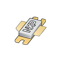
BLF6G20-110 NXP Semiconductors, BLF6G20-110 Datasheet

BLF6G20-110
Specifications of BLF6G20-110
Available stocks
Related parts for BLF6G20-110
BLF6G20-110 Summary of contents
Page 1
... BLF6G20-110; BLF6G20LS-110 Power LDMOS transistor Rev. 03 — 13 January 2009 1. Product profile 1.1 General description 110 W LDMOS power transistor for base station applications at frequencies from 1800 MHz to 2000 MHz. Table 1. RF performance at T Mode of operation 2-carrier W-CDMA [1] Test signal: 3GPP; test model 1; 64 DPCH; PAR = 0.01 % probability on CCDF per carrier; carrier spacing 10 MHz ...
Page 2
... NXP Semiconductors 1.3 Applications I RF power amplifiers for GSM, GSM EDGE, W-CDMA and CDMA base stations and multicarrier applications in the 1800 MHz to 2000 MHz frequency range 2. Pinning information Table 2. Pin BLF6G20-110 (SOT502A BLF6G20LS-110 (SOT502B [1] Connected to flange. 3. Ordering information Table 3. Type number ...
Page 3
... RF performance at V class-AB production test circuit. Symbol P L(AV IMD3 ACPR 7.1 Ruggedness in class-AB operation The BLF6G20-110 and BLF6G20LS-110 are capable of withstanding a load mismatch corresponding to VSWR = through all phases under the following conditions BLF6G20-110_BLF6G20LS-110_3 Product data sheet BLF6G20-110; BLF6G20LS-110 Thermal characteristics Parameter Conditions ...
Page 4
... G p (dB 1400 mA 1960 MHz Fig 2. Two-tone CW power gain and drain efficiency as function of peak envelope load power; typical values BLF6G20-110_BLF6G20LS-110_3 Product data sheet BLF6G20-110; BLF6G20LS-110 (dB 1400 mA 1960 MHz One-tone CW power gain and drain efficiency as function of load power; typical values 001aaj073 60 D IMD3 ...
Page 5
... BLF6G20-110 or BLF6G20LS-110 SMD resistor SMD resistor Rev. 03 — 13 January 2009 Power LDMOS transistor C3 C10 ...
Page 6
... D UNIT 4.72 12.83 20.02 0.15 mm 3.43 12.57 0.08 19.61 0.186 0.505 0.006 0.788 inches 0.495 0.135 0.003 0.772 OUTLINE VERSION IEC SOT502A Fig 5. Package outline SOT502A BLF6G20-110_BLF6G20LS-110_3 Product data sheet BLF6G20-110; BLF6G20LS-110 scale 19.96 9.50 9.53 1.14 19.94 5.33 19.66 9 ...
Page 7
... UNIT 4.72 12.83 20.02 0.15 mm 3.43 12.57 0.08 19.61 0.186 0.505 0.006 0.788 inches 0.495 0.135 0.003 0.772 OUTLINE VERSION IEC SOT502B Fig 6. Package outline SOT502B BLF6G20-110_BLF6G20LS-110_3 Product data sheet BLF6G20-110; BLF6G20LS-110 scale 19.96 9.50 9.53 1.14 19.94 5.33 19.66 9.30 9 ...
Page 8
... Revision history Document ID BLF6G20-110_BLF6G20LS-110_3 20090113 Modifications: BLF6G20-110_BLF6G20LS-110_2 20081117 BLF6G20-110_BLF6G20LS-110_1 20080128 BLF6G20-110_BLF6G20LS-110_3 Product data sheet BLF6G20-110; BLF6G20LS-110 Abbreviations Description Third Generation Partnership Project Complementary Cumulative Distribution Function Code Division Multiple Access Continuous Wave Dedicated Physical CHannel Enhanced Data rates for GSM Evolution ...
Page 9
... For more information, please visit: For sales office addresses, please send an email to: BLF6G20-110_BLF6G20LS-110_3 Product data sheet BLF6G20-110; BLF6G20LS-110 [3] Definition This document contains data from the objective specification for product development. This document contains data from the preliminary specification. ...
Page 10
... NXP B.V. 2009. For more information, please visit: http://www.nxp.com For sales office addresses, please send an email to: salesaddresses@nxp.com Power LDMOS transistor All rights reserved. Date of release: 13 January 2009 Document identifier: BLF6G20-110_BLF6G20LS-110_3 ...


