NDS9952A Fairchild Semiconductor, NDS9952A Datasheet
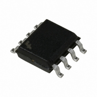
MOSFET N+P 30V 2.9A 8-SOIC

NDS9952A

Manufacturer Part Number
NDS9952A
Description
MOSFET N+P 30V 2.9A 8-SOIC
Manufacturer
Fairchild Semiconductor
Type
Power MOSFETr
Datasheet

Specifications of NDS9952A

Fet Type
N and P-Channel
Fet Feature
Logic Level Gate
Rds On (max) @ Id, Vgs
80 mOhm @ 1A, 10V
Drain To Source Voltage (vdss)
30V
Current - Continuous Drain (id) @ 25° C
3.7A, 2.9A
Vgs(th) (max) @ Id
2.8V @ 250µA
Gate Charge (qg) @ Vgs
25nC @ 10V
Input Capacitance (ciss) @ Vds
320pF @ 10V
Power - Max
900mW
Mounting Type
Surface Mount
Package / Case
8-SOIC (3.9mm Width)
Transistor Polarity
N And P Channel
Continuous Drain Current Id
3.7A
Drain Source Voltage Vds
30V
On Resistance Rds(on)
80mohm
Rds(on) Test Voltage Vgs
10V
Threshold Voltage Vgs Typ
1.7V
Rohs Compliant
Yes
Number Of Elements
2
Polarity
N/P
Channel Mode
Enhancement
Drain-source On-volt
30V
Gate-source Voltage (max)
±20V
Power Dissipation
2W
Operating Temp Range
-55C to 150C
Operating Temperature Classification
Military
Mounting
Surface Mount
Pin Count
8
Package Type
SOIC N
Lead Free Status / RoHS Status
Lead free / RoHS Compliant
Other names
NDS9952ATR

Available stocks

Company
Part Number
Manufacturer
Quantity
Price
Part Number:
NDS9952A
Manufacturer:
FSC
Quantity:
47 500
Part Number:
NDS9952A
Manufacturer:
NS
Quantity:
1 103
Part Number:
NDS9952A
Manufacturer:
FSC
Quantity:
50 000
Part Number:
NDS9952A
Manufacturer:
FSC
Quantity:
111
Part Number:
NDS9952A
Manufacturer:
NS/国半
Quantity:
20 000
Company:
Part Number:
NDS9952A
Quantity:
300
Part Number:
NDS9952A-NL
Manufacturer:
FAIRCHILD/仙童
Quantity:
20 000
Absolute Maximum Ratings
Symbol
V
V
I
P
T
THERMAL CHARACTERISTICS
R
R
________________________________________________________________________________
D
© 1997 Fairchild Semiconductor Corporation
J
NDS9952A
Dual N & P-Channel Enhancement Mode Field Effect Transistor
DSS
GSS
D
These dual N- and P-channel enhancement mode power
field effect transistors are produced using Fairchild's
proprietary, high cell density, DMOS technology. This
very high density process is especially tailored to
minimize on-state resistance, provide superior switching
performance, and withstand high energy pulses in the
avalanche and commutation modes. These devices are
particularly suited for low voltage applications such as
notebook computer power management
battery powered circuits where fast switching, low in-line
power loss, and resistance to transients are needed.
,T
General Description
JA
JC
STG
Parameter
Drain-Source Voltage
Gate-Source Voltage
Drain Current - Continuous
Power Dissipation for Dual Operation
Power Dissipation for Single Operation
Operating and Storage Temperature Range
Thermal Resistance, Junction-to-Ambient
Thermal Resistance, Junction-to-Case
- Pulsed
T
A
= 25°C unless otherwise noted
and other
(Note 1a)
(Note 1a)
(Note 1c)
(Note 1b)
(Note 1a)
(Note 1)
Features
N-Channel 3.7A, 30V, R
P-Channel -2.9A, -30V, R
High density cell design or extremely low R
High power and current handling capability in a widely used
surface mount package.
Dual (N & P-Channel) MOSFET in surface mount package.
N-Channel
± 3.7
± 20
± 15
30
6
5
8
7
-55 to 150
1.6
0.9
78
40
2
1
DS(ON)
DS(ON)
=0.08
=0.13
P-Channel
± 2.9
± 20
± 10
-30
@ V
@ V
4
3
2
1
GS
DS(ON)
GS
February 1996
=10V.
=-10V.
.
NDS9952A.SAM
Units
°C/W
°C/W
W
°C
V
V
A

Related parts for NDS9952A

NDS9952A Summary of contents

Page 1

... T = 25°C unless otherwise noted A N-Channel 30 ± 20 ± 3.7 (Note 1a) ± 15 (Note 1a) (Note 1b) (Note 1c) (Note 1a) (Note 1) February 1996 =0. =10V. DS(ON) GS =0. =-10V. DS(ON DS(ON P-Channel -30 ± 20 ± 2.9 ± 1.6 1 0.9 -55 to 150 78 40 Units °C °C/W °C/W NDS9952A.SAM ...

Page 2

... P-Ch -1 -1.6 -2.8 -0.85 -1.25 -2.5 N-Ch 0.06 0.08 0.08 0.13 0.08 0.11 0.11 0.18 P-Ch 0.11 0.13 0.15 0.21 0.17 0.2 0.24 0.32 N- P-Ch -10 N- P-Ch 4 N-Ch 320 pF P-Ch 350 N-Ch 225 pF P-Ch 260 N- P-Ch 100 NDS9952A.SAM ...

Page 3

... A/µ -1. /dt = 100 A/µ Type Min Typ Max Units N-Ch 9 N-Ch 1.5 P-Ch 1.6 N-Ch 3.3 P-Ch 3.4 N-Ch 1.2 P-Ch -1.2 N-Ch 0.8 1.3 P-Ch -0.8 -1.3 N-Ch 75 P-Ch 100 is guaranteed NDS9952A.SAM ...

Page 4

... Figure 6. N-Channel Gate Threshold Variation V = 3.5V GS 4.0 4.5 5 DRAIN CURRENT (A) D Gate Voltage and Drain Current 125°C J 25° DRAIN CURRENT (A) D Drain Current and Temperature 250µ JUNCTION TEMPERATURE (°C) J with Temperature. 6.0 8 -55° NDS9952A.SAM ...

Page 5

... C iss 6 C oss rss Figure 10. N-Channel Gate Charge Characteristics -55°C J 25°C 125° 125°C J 25°C -55°C 0.4 0.6 0 BODY DIODE FORWARD VOLTAGE (V) SD Variation with Current and Temperature V = 10V DS 20V GATE CHARGE (nC) g 1.4 . 15V 12 NDS9952A.SAM ...

Page 6

... GS -4.0 -4.5 -5.0 -5 DRAIN CURRENT (A) D Gate Voltage and Drain Current. = -10V 125°C J 25° - DRAIN CURRENT (A) D Drain Current and Temperature -250µ 100 T , JUNCTION TEMPERATURE (°C) J with Temperature. -7.0 -8.0 -10 -15 -55°C -15 GS 125 150 NDS9952A.SAM ...

Page 7

... C iss 6 C oss rss Figure 21. P-Channel Gate Charge Characteristics. 25°C 125° - 125°C J 25°C -55°C 0.4 0.6 0 BODY DIODE FORWARD VOLTAGE (V) SD Voltage Variation with Current and Temperature . V = -10V = -2. GATE CHARGE (nC) g 1.4 -20V -15V 12 NDS9952A.SAM ...

Page 8

... V 0.1 SINGLE PULSE 4.5"x5" FR-4 Board 0. Still Air 0. 0.1 0.2 0.4 0 Figure 26. N-Channel Maximum Safe Operating Area 4.5"x5" FR-4 Board Still Air 0.1 0.2 0.3 0.4 2 2oz COPPER MOUNTING PAD AREA ( 10V GS = See Note 1c = 25° DRAIN-SOURCE VOLTAGE ( 0 NDS9952A.SAM ...

Page 9

... Note: Thermal characterization performed using the conditions described in note 1c. Transient thermal response will change depending on the circuit board design GEN G S Figure 29 P-Channel Switching Test Circuit TIME (sec d(on OUT DUT Figure 30 P-Channel Switching Waveforms R ( See Note 1c JA P(pk ( Duty Cycle d(off PULSE WIDTH NDS9952A.SAM ...

Page 10

... TRADEMARKS The following are registered and unregistered trademarks Fairchild Semiconductor owns or is authorized to use and is not intended exhaustive list of all such trademarks. ACEx™ Bottomless™ CoolFET™ CROSSVOLT™ CMOS FACT™ FACT Quiet Series™ FAST FASTr™ GTO™ ...

Related keywords