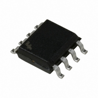
NDS9952A Fairchild Semiconductor, NDS9952A Datasheet - Page 3

NDS9952A
Manufacturer Part Number
NDS9952A
Description
MOSFET N+P 30V 2.9A 8-SOIC
Manufacturer
Fairchild Semiconductor
Type
Power MOSFETr
Datasheet
1.NDS9952A.pdf
(10 pages)
Specifications of NDS9952A
Fet Type
N and P-Channel
Fet Feature
Logic Level Gate
Rds On (max) @ Id, Vgs
80 mOhm @ 1A, 10V
Drain To Source Voltage (vdss)
30V
Current - Continuous Drain (id) @ 25° C
3.7A, 2.9A
Vgs(th) (max) @ Id
2.8V @ 250µA
Gate Charge (qg) @ Vgs
25nC @ 10V
Input Capacitance (ciss) @ Vds
320pF @ 10V
Power - Max
900mW
Mounting Type
Surface Mount
Package / Case
8-SOIC (3.9mm Width)
Transistor Polarity
N And P Channel
Continuous Drain Current Id
3.7A
Drain Source Voltage Vds
30V
On Resistance Rds(on)
80mohm
Rds(on) Test Voltage Vgs
10V
Threshold Voltage Vgs Typ
1.7V
Rohs Compliant
Yes
Number Of Elements
2
Polarity
N/P
Channel Mode
Enhancement
Drain-source On-volt
30V
Gate-source Voltage (max)
±20V
Power Dissipation
2W
Operating Temp Range
-55C to 150C
Operating Temperature Classification
Military
Mounting
Surface Mount
Pin Count
8
Package Type
SOIC N
Lead Free Status / RoHS Status
Lead free / RoHS Compliant
Other names
NDS9952ATR
Available stocks
Company
Part Number
Manufacturer
Quantity
Price
Company:
Part Number:
NDS9952A
Manufacturer:
FSC
Quantity:
47 500
Company:
Part Number:
NDS9952A
Manufacturer:
NS
Quantity:
1 103
Company:
Part Number:
NDS9952A
Manufacturer:
FSC
Quantity:
50 000
Part Number:
NDS9952A
Manufacturer:
NS/ه›½هچٹ
Quantity:
20 000
Part Number:
NDS9952A-NL
Manufacturer:
FAIRCHILD/ن»™ç«¥
Quantity:
20 000
Symbol
SWITCHING CHARACTERISTICS
t
t
t
t
Q
Q
Q
DRAIN-SOURCE DIODE CHARACTERISTICS AND MAXIMUM RATINGS
I
V
t
Notes:
Electrical Characteristics
D(on)
r
D(off)
f
S
rr
1. R
2. Pulse Test: Pulse Width < 300µs, Duty Cycle < 2.0%.
SD
g
gs
gd
P
design while R
Typical R
D
JA
t
is the sum of the junction-to-case and case-to-ambient thermal resistance where the case thermal reference is defined as the solder mounting surface of the drain pins. R
R
T
a. 78
b. 125
c. 135
Scale 1 : 1 on letter size paper
JA
1a
J
J A
for single device operation using the board layouts shown below on 4.5"x5" FR-4 PCB in a still air environment:
T
A
Parameter
Turn - On Delay Time
Turn - On Rise Time
Turn - Off Delay Time
Turn - Off Fall Time
Total Gate Charge
Gate-Source Charge
Gate-Drain Charge
Maximum Continuous Drain-Source Diode Forward Current
Drain-Source Diode Forward
Voltage
Reverse Recovery Time
t
o
CA
C/W when mounted on a 0.5 in
o
o
C/W when mounted on a 0.02 in
C/W when mounted on a 0.003 in
is determined by the user's board design.
R
J C
T
J
R
T
A
CA
t
I
2
D
t
R
2
DS ON
pad of 2oz cpper.
(Note 2)
(T
2
pad of 2oz cpper.
2
pad of 2oz cpper.
A
= 25°C unless otherwise noted)
T
J
Conditions
N-Channel
V
V
P-Channel
V
V
N-Channel
V
I
P-Channel
V
I
V
V
V
V
D
D
DD
GEN
DD
GEN
DS
DS
GS
GS
GS
GS
1b
= 3.7 A, V
= -2.9 A, V
= 10 V,
= -10 V,
= 10 V, I
= -10 V, I
= 0 V, I
= 0 V, I
= 0 V, I
= 0 V, I
= 10 V, R
= -10 V, R
F
F
S
S
= 1.25 A, dI
= -1.25 A, dI
D
= 1.25 A
= -1.25 A
D
GS
GS
GEN
= 1 A,
GEN
= -1 A,
= 10 V
= -10 V
= 6
= 6
(Note 2)
(Note 2)
F
/dt = 100 A/µs
F
/dt = 100 A/µs
1c
Type
N-Ch
P-Ch
N-Ch
P-Ch
N-Ch
P-Ch
N-Ch
P-Ch
N-Ch
P-Ch
N-Ch
P-Ch
N-Ch
P-Ch
N-Ch
P-Ch
N-Ch
P-Ch
N-Ch
P-Ch
Min
Typ
-0.8
9.5
1.5
1.6
3.3
3.4
0.8
10
13
21
21
21
10
9
5
8
JC
Max
-1.2
-1.3
100
1.2
1.3
15
40
20
40
50
90
50
50
27
25
75
is guaranteed by
NDS9952A.SAM
Units
nC
nC
nC
ns
ns
ns
ns
ns
A
V


