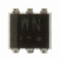
RTL030P02TR Rohm Semiconductor, RTL030P02TR Datasheet - Page 2

RTL030P02TR
Manufacturer Part Number
RTL030P02TR
Description
MOSFET P-CH 20V 3A TUMT6
Manufacturer
Rohm Semiconductor
Datasheet
1.RTL030P02TR.pdf
(5 pages)
Specifications of RTL030P02TR
Fet Type
MOSFET P-Channel, Metal Oxide
Fet Feature
Logic Level Gate
Rds On (max) @ Id, Vgs
70 mOhm @ 3A, 4.5V
Drain To Source Voltage (vdss)
20V
Current - Continuous Drain (id) @ 25° C
3A
Vgs(th) (max) @ Id
2V @ 1mA
Gate Charge (qg) @ Vgs
8nC @ 4.5V
Input Capacitance (ciss) @ Vds
760pF @ 10V
Power - Max
1W
Mounting Type
Surface Mount
Package / Case
TUMT6
Configuration
Single Quad Drain
Transistor Polarity
P-Channel
Resistance Drain-source Rds (on)
0.07 Ohm @ 4.5 V
Drain-source Breakdown Voltage
20 V
Gate-source Breakdown Voltage
+/- 12 V
Continuous Drain Current
3 A
Power Dissipation
1000 mW
Mounting Style
SMD/SMT
Lead Free Status / RoHS Status
Lead free / RoHS Compliant
Available stocks
Company
Part Number
Manufacturer
Quantity
Price
Part Number:
RTL030P02TR
Manufacturer:
ROHM/罗姆
Quantity:
20 000
Transistors
! ! ! ! Absolute maximum ratings (Ta=25 C)
! ! ! ! Electrical characteristics (Ta=25 C)
Drain-source voltage
Gate-source voltage
Drain current
Total power dissipation
Channel temperature
Range of Storage temperature
Source current
(Body diode)
1 Pw 10 s, Duty cycle 1%
2 Mounted on a ceramic board
Pulsed
Gate-source leakage
Drain-source breakdown voltage
Zero gate voltage drain current
Gate threshold voltage
Static drain-source on-state
resistance
Forward transfer admittance
Input capacitance
Output capacitance
Reverse transfer capacitance
Turn-on delay time
Rise time
Turn-off delay time
Fall time
Total gate charge
Gate-source charge
Gate-drain charge
Body diode characteristics (source-drain characteristics)
Forward voltage
Parameter
Parameter
V
Symbol
Continuous
Pulsed
Continuous
Pulsed
R
V
(BR) DSS
t
t
VSD
C
I
I
C
GS (th)
DS (on)
C
d (on)
d (off)
Q
Q
Y
GSS
DSS
Q
t
t
oss
iss
rss
gd
fs
r
f
gs
g
Min.
2.0
0.7
20
Symbol
V
V
Tstg
Tch
I
I
P
DSS
GSS
I
DP
I
SP
D
S
D
Typ.
760
125
100
8.0
1.5
2.5
50
55
90
12
25
50
22
Max.
125
70
77
2.0
1.2
10
55 to 150
1
Limits
150
0.8
20
12
12
12
1
3
Unit
m
m
m
nC
nC
nC
pF
pF
pF
ns
ns
ns
ns
V
V
S
V
A
A
V
I
V
V
I
I
I
V
V
V
f=1MHz
I
V
V
R
R
V
V
I
D
D
D
D
D
D
I
S
GS
DS
DS
DS
DS
GS
DD
GS
L
GS
DD
GS
= 1mA, V
= 3.0A, V
= 3.0A, V
= 1.5A, V
= 1.5A
= 3A
= 0.8A, V
=10
= 20V, V
= 10V, I
= 10V, I
= 10V
= 12V, V
=0V
= 4.5V
=10
= 4.5V
15V
15 V
Unit
W
V
V
A
A
A
A
C
C
Conditions
GS
GS
GS
GS
D
D
GS
DS
GS
= 1mA
= 1.5A
R
R
=0V
= 4.5V
= 4V
= 2.5V
=0V
=0V
L
GS
=0V
1
1
2
=10
5
RTL030P02
2/4


