NTD4810N-35G ON Semiconductor, NTD4810N-35G Datasheet

MOSFET N-CH 30V 8.6A IPAK

NTD4810N-35G

Manufacturer Part Number
NTD4810N-35G
Description
MOSFET N-CH 30V 8.6A IPAK
Manufacturer
ON Semiconductor
Datasheet

Specifications of NTD4810N-35G

Fet Type
MOSFET N-Channel, Metal Oxide
Fet Feature
Logic Level Gate
Rds On (max) @ Id, Vgs
10 mOhm @ 30A, 10V
Drain To Source Voltage (vdss)
30V
Current - Continuous Drain (id) @ 25° C
8.6A
Vgs(th) (max) @ Id
2.5V @ 250µA
Gate Charge (qg) @ Vgs
11nC @ 4.5V
Input Capacitance (ciss) @ Vds
1350pF @ 12V
Power - Max
1.28W
Mounting Type
Through Hole
Package / Case
IPak, TO-251, DPak (3 straight short leads + tab)
Configuration
Single
Transistor Polarity
N-Channel
Resistance Drain-source Rds (on)
0.01 Ohms
Drain-source Breakdown Voltage
30 V
Gate-source Breakdown Voltage
+/- 20 V
Continuous Drain Current
10.8 A
Power Dissipation
2 W
Maximum Operating Temperature
+ 175 C
Mounting Style
Through Hole
Minimum Operating Temperature
- 55 C
Lead Free Status / RoHS Status
Lead free / RoHS Compliant

Available stocks

Company
Part Number
Manufacturer
Quantity
Price
Part Number:
NTD4810N-35G
Manufacturer:
ON
Quantity:
12 500
NTD4810N
Power MOSFET
30 V, 54 A, Single N- -Channel, DPAK/IPAK
Features
Applications
Stresses exceeding Maximum Ratings may damage the device. Maximum
Ratings are stress ratings only. Functional operation above the Recommended
Operating Conditions is not implied. Extended exposure to stresses above the
Recommended Operating Conditions may affect device reliability.
MAXIMUM RATINGS
© Semiconductor Components Industries, LLC, 2010
June, 2010 - - Rev. 8
Continuous Drain
Current (R
Power Dissipation
(R
Continuous Drain
Current (R
Power Dissipation
(R
Continuous Drain
Current (R
(Note 1)
Power Dissipation
(R
Pulsed Drain Current
Current Limited by Package
Operating Junction and Storage Temperature
Source Current (Body Diode)
Drain to Source dV/dt
Single Pulse Drain--to--Source Avalanche
Energy (V
L = 1.0 mH, I
Lead Temperature for Soldering Purposes
(1/8″ from case for 10 s)
Drain--to--Source Voltage
Gate--to--Source Voltage
Low R
Low Capacitance to Minimize Driver Losses
Optimized Gate Charge to Minimize Switching Losses
These are Pb- -Free Devices
CPU Power Delivery
DC- -DC Converters
θJA
θJA
θJC
) (Note 1)
) (Note 2)
) (Note 1)
DS(on)
DD
θJA
θJA
θJC
L(pk)
= 24 V, V
) (Note 1)
) (Note 2)
)
to Minimize Conduction Losses
Parameter
= 14 A, R
GS
(T
t
= 10 V,
J
Steady
p
State
G
=10ms
= 25°C unless otherwise noted)
= 25 Ω)
T
T
T
T
T
T
T
T
T
T
T
A
A
A
A
A
A
C
C
C
A
A
= 25°C
= 85°C
= 25°C
= 25°C
= 85°C
= 25°C
= 25°C
= 85°C
= 25°C
= 25°C
= 25°C
I
Symbol
DmaxPkg
T
V
dV/dt
J
V
E
I
P
P
P
, T
T
DSS
DM
I
I
I
I
GS
D
D
D
AS
S
D
D
D
L
stg
-- 55 to
Value
20
10.8
1.28
120
175
260
8.4
2.0
8.6
6.7
6.0
30
54
42
50
45
41
98
1
V/ns
Unit
mJ
°C
°C
W
W
W
V
V
A
A
A
A
A
A
Gate
See detailed ordering and shipping information in the package
dimensions section on page 6 of this data sheet.
1
CASE 369AA
(Bent Lead)
V
1 2
Drain
Drain 3
(BR)DSS
STYLE 2
30 V
DPAK
4
2
3
Source
ORDERING INFORMATION
G
Y
WW
4810N = Device Code
G
MARKING DIAGRAMS
& PIN ASSIGNMENTS
4
http://onsemi.com
Gate
15.7 mΩ @ 4.5 V
(Straight Lead)
10 mΩ @ 10 V
CASE 369AC
R
1
= Year
= Work Week
= Pb--Free Package
Drain
DS(on)
Drain
3 IPAK
D
1
4
2
2 3
Publication Order Number:
3
S
Source
MAX
4
Gate
N- -Channel
(Straight Lead
CASE 369D
1
NTD4810N/D
1
Drain
Drain
DPAK)
2
IPAK
4
I
D
2
3
54 A
MAX
3
Source
4

Related parts for NTD4810N-35G

NTD4810N-35G Summary of contents

Page 1

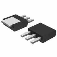
... CASE 369AC CASE 369D 3 IPAK IPAK (Straight Lead) (Straight Lead DPAK) MARKING DIAGRAMS & PIN ASSIGNMENTS 4 Drain 4 Drain Gate Drain Source Source Gate Drain Source Y = Year WW = Work Week 4810N = Device Code G = Pb--Free Package ORDERING INFORMATION Publication Order Number: NTD4810N/D ...

Page 2

THERMAL RESISTANCE MAXIMUM RATINGS Junction--to--Case (Drain) Junction--to--TAB (Drain) Junction--to--Ambient -- Steady State (Note 1) Junction--to--Ambient -- Steady State (Note 2) 1. Surface--mounted on FR4 board using pad size Cu. 2. Surface--mounted on FR4 board using ...

Page 3

ELECTRICAL CHARACTERISTICS Parameter DRAIN- -SOURCE DIODE CHARACTERISTICS Forward Diode Voltage Reverse Recovery Time Charge Time Discharge Time Reverse Recovery Time PACKAGE PARASITIC VALUES Source Inductance Drain Inductance, DPAK Drain Inductance, IPAK Gate Inductance Gate Resistance (T = 25°C unless otherwise ...

Page 4

25° 4 DRAIN--TO--SOURCE VOLTAGE (VOLTS) DS Figure 1. On- -Region Characteristics 0.048 0.043 0.038 0.033 ...

Page 5

iss 1500 1000 C rss 500 C rss GATE--TO--SOURCE OR DRAIN--TO--SOURCE VOLTAGE (VOLTS) Figure 7. Capacitance Variation 1000 ...

Page 6

... ORDERING INFORMATION Order Number NTD4810NT4G NTD4810N--1G NTD4810N--35G †For information on tape and reel specifications, including part orientation and tape sizes, please refer to our Tape and Reel Packaging Specifications Brochure, BRD8011/D. TYPICAL PERFORMANCE CURVES 25°C 100°C 125°C ...

Page 7

... DETAIL 0.005 (0.13 *For additional information on our Pb--Free strategy and soldering details, please download the ON Semiconductor Soldering and Mounting Techniques Reference Manual, SOLDERRM/D. PACKAGE DIMENSIONS DPAK (SINGLE GUAGE) CASE 369AA--01 ISSUE GAUGE L2 SEATING C PLANE PLANE DETAIL A ROTATED 90 CW ° SOLDERING FOOTPRINT* 6 ...

Page 8

... R 0.180 0.215 4.45 5.45 S 0.025 0.040 0.63 1.01 V 0.035 0.050 0.89 1.27 Z 0.155 ------ 3.93 ------ STYLE 2: PIN 1. GATE 2. DRAIN 3. SOURCE 4. DRAIN ON Semiconductor Website: www.onsemi.com Order Literature: http://www.onsemi.com/orderlit For additional information, please contact your local Sales Representative NTD4810N/D ...

Related keywords