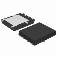
NTMFS4833NT1G ON Semiconductor, NTMFS4833NT1G Datasheet - Page 2

NTMFS4833NT1G
Manufacturer Part Number
NTMFS4833NT1G
Description
MOSFET N-CH 30V 16A SO-8FL
Manufacturer
ON Semiconductor
Type
Power MOSFETr
Specifications of NTMFS4833NT1G
Fet Type
MOSFET N-Channel, Metal Oxide
Fet Feature
Logic Level Gate
Rds On (max) @ Id, Vgs
2 mOhm @ 30A, 10V
Drain To Source Voltage (vdss)
30V
Current - Continuous Drain (id) @ 25° C
16A
Vgs(th) (max) @ Id
2.5V @ 250µA
Gate Charge (qg) @ Vgs
58nC @ 4.5V
Input Capacitance (ciss) @ Vds
5600pF @ 12V
Power - Max
910mW
Mounting Type
Surface Mount
Package / Case
5-DFN, SO8 FL
Configuration
Single
Transistor Polarity
N-Channel
Resistance Drain-source Rds (on)
2.3 m Ohms
Forward Transconductance Gfs (max / Min)
30 S
Drain-source Breakdown Voltage
30 V
Gate-source Breakdown Voltage
20 V
Continuous Drain Current
191 A
Power Dissipation
125 W
Maximum Operating Temperature
+ 150 C
Mounting Style
SMD/SMT
Minimum Operating Temperature
- 55 C
Number Of Elements
1
Polarity
N
Channel Mode
Enhancement
Drain-source On-res
0.002Ohm
Drain-source On-volt
30V
Gate-source Voltage (max)
20V
Operating Temp Range
-55C to 150C
Operating Temperature Classification
Military
Mounting
Surface Mount
Pin Count
8
Package Type
SO-FL
Lead Free Status / RoHS Status
Lead free / RoHS Compliant
Other names
NTMFS4833NT1G
NTMFS4833NT1GOSTR
NTMFS4833NT1GOSTR
Available stocks
Company
Part Number
Manufacturer
Quantity
Price
Company:
Part Number:
NTMFS4833NT1G
Manufacturer:
ON
Quantity:
721
Part Number:
NTMFS4833NT1G
Manufacturer:
ON/安森美
Quantity:
20 000
3. Surface-mounted on FR4 board using 1 sq-in pad, 1 oz Cu.
4. Surface-mounted on FR4 board using the minimum recommended pad size.
THERMAL RESISTANCE MAXIMUM RATINGS
ELECTRICAL CHARACTERISTICS
OFF CHARACTERISTICS
ON CHARACTERISTICS (Note 5)
CHARGES, CAPACITANCES & GATE RESISTANCE
SWITCHING CHARACTERISTICS (Note 6)
5. Pulse Test: pulse width v 300 ms, duty cycle v 2%.
6. Switching characteristics are independent of operating junction temperatures.
Junction-to-Case (Drain)
Junction-to-Ambient – Steady State (Note 3)
Junction-to-Ambient – Steady State (Note 4)
Drain-to-Source Breakdown Voltage
Drain-to-Source Breakdown Voltage
Temperature Coefficient
Zero Gate Voltage Drain Current
Gate-to-Source Leakage Current
Gate Threshold Voltage
Negative Threshold Temperature Coefficient
Drain-to-Source On Resistance
Forward Transconductance
Input Capacitance
Output Capacitance
Reverse Transfer Capacitance
Total Gate Charge
Threshold Gate Charge
Gate-to-Source Charge
Gate-to-Drain Charge
Total Gate Charge
Turn-On Delay Time
Rise Time
Turn-Off Delay Time
Fall Time
Turn-On Delay Time
Rise Time
Turn-Off Delay Time
Fall Time
Parameter
Parameter
(T
J
= 25°C unless otherwise specified)
V
V
V
Symbol
Q
Q
V
GS(TH)
(BR)DSS
R
t
t
(BR)DSS
Q
t
t
d(OFF)
d(OFF)
C
C
I
I
d(ON)
d(ON)
GS(TH)
C
G(TOT)
Q
Q
G(TOT)
DSS
GSS
DS(on)
g
G(TH)
T
OSS
RSS
t
t
t
t
ISS
FS
GD
GS
r
f
r
f
J
/T
http://onsemi.com
/
J
NTMFS4833N
V
V
V
GS
GS
GS
V
V
V
V
V
GS
V
= 4.5 V, V
2
= 4.5 V, V
V
DS
GS
= 0 V, f = 1 MHz, V
V
V
GS
GS
GS
I
V
DS
11.5 V
D
GS
GS
= 10 V to
DS
= 24 V
= 4.5 V
= 0 V,
= 11.5 V, V
= 15 A, R
= 11.5 V, V
Test Condition
= 0 V, V
= 0 V, I
= V
= 15 V, I
R
Symbol
I
G
R
R
R
D
DS
DS
DS
qJC
qJA
qJA
= 3.0 W
= 30 A
, I
= 15 V, I
D
= 15 V; I
GS
D
G
= 250 mA
D
DS
DS
= 250 mA
= 3.0 W
= ±20 V
= 15 A
= 15 V,
= 15 V;
T
T
DS
I
I
I
I
J
J
D
D
D
D
D
D
= 125°C
= 25 °C
= 15 A,
= 30 A
= 15 A
= 30 A
= 15 A
= 12 V
= 30 A
Value
137.8
53.2
1.0
Min
30
1.5
5600
1200
Typ
7.12
650
17
1.3
1.3
2.3
2.3
6.0
25
34
35
17
14
19
50
10
30
39
16
17
88
±100
Max
10
2.5
2.0
3.0
58
1
°C/W
Unit
mV/°C
mV/°C
Unit
mA
nA
mW
ns
ns
nC
nC
pF
V
V
S


