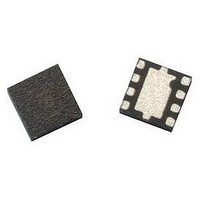
ATF-521P8-TR2 Avago Technologies US Inc., ATF-521P8-TR2 Datasheet - Page 18

ATF-521P8-TR2
Manufacturer Part Number
ATF-521P8-TR2
Description
IC PHEMT 2GHZ 4.5V 200MA 8-LPCC
Manufacturer
Avago Technologies US Inc.
Datasheet
1.ATF-521P8-BLK.pdf
(23 pages)
Specifications of ATF-521P8-TR2
Gain
17dB
Transistor Type
pHEMT FET
Frequency
2GHz
Voltage - Rated
7V
Current Rating
500mA
Noise Figure
1.5dB
Current - Test
200mA
Voltage - Test
4.5V
Power - Output
26.5dBm
Package / Case
8-LPCC
Drain Source Voltage Vds
4.5V
Continuous Drain Current Id
500mA
Power Dissipation Pd
1.5W
Noise Figure Typ
1.5dB
Rf Transistor Case
LPCC
No. Of Pins
8
Frequency Max
6GHz
Frequency Min
50MHz
Drain Current Idss Max
200mA
Rohs Compliant
Yes
Lead Free Status / RoHS Status
Lead free / RoHS Compliant
Available stocks
Company
Part Number
Manufacturer
Quantity
Price
Part Number:
ATF-521P8-TR2
Manufacturer:
AVAGO/安华高
Quantity:
20 000
Figure 13. ATF-521P8 Matching.
As described previously the input impedance must
be matched to S11* in order to guarantee return loss
greater than 10 dB. A high pass network is chosen for
this match. The output is matched to Γ
high pass network. The next step is to choose the
proper DC biasing conditions. From the data sheet,
ATF‑521P8 produces good linearity at a drain current
of 200mA and a drain to source voltage of 4.5V. Thus to
construct the active bias circuit described, the following
parameters are given:
Ids = 200 mA
I
V
V
V
V
Using equations 4, 5, 6, and 7, the biasing resistor values
are calculated in column 2 of table 1, and the actual
values used are listed in column 3.
RF
Figure 14. 2140 MHz Schematic.
18
R
dd
ds
g
be1
= 10 mA
in
= 0.62V
50 Ohm
= 4.5V
= 5 V
= 0.65 V
Match
Input
S11* = 0.89∠ -169
C1=1.2pF
C2=1.5nH
C3=4.7pF
C4=1µF
R4=61.9Ω
R2=383Ω
2PL
L2=12nH
R5=10Ω
L1=1.0nH
Γ
L
I
V
R
= 0.53∠ -176
g
Output
Match
I
50 Ohm
Q1
Q2
C2
ATF-521P8
2
R6=1.2Ω
2PL
V
V
be1 +
ds
R1=49.9Ω
R3=2.37Ω
7
C7=150pF
C6=.1µF
L3=39nH
L
C8=1.5pF
with another
C5=1µF
+5V
L4=3.9nH
RF
Table 1. Resistors for Active Bias.
Resistor
R1
R2
R3
R4
The entire circuit schematic for a 2.14 GHz Tx driver
amplifier is shown below in Figure 14. Capacitors C4,
C5, and C6 are added as a low frequency bypass. These
terminate second order harmonics and help improve
linearity. Resistors R5 and R6 also help terminate low
frequencies, and can prevent resonant frequencies
between the two bypass capacitors.
Performance of ATF-521P8 at 2140 MHz
ATF‑521P8 delivers excellent performance in the
WCDMA frequency band. With a drain‑to‑source voltage
of 4.5V and a drain current of 200 mA, this device has
16.5 dB of gain and 1.55 dB of noise figure as show in
Figure 15.
ou t
Calculated
50Ω
385Ω
2.38Ω
62Ω
Actual
49.9Ω
383Ω
2.37Ω
61.9Ω


