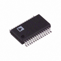
AD9851BRS Analog Devices Inc, AD9851BRS Datasheet - Page 11

AD9851BRS
Manufacturer Part Number
AD9851BRS
Description
Direct Digital Synthesizer 180MHz 1-DAC 10-Bit Parallel/Serial 28-Pin SSOP
Manufacturer
Analog Devices Inc
Datasheet
1.AD9851BRSZ.pdf
(24 pages)
Specifications of AD9851BRS
Resolution
10 Bit
Maximum Input Frequency
180 MHz
Tuning Word Width
32 Bit
Minimum Operating Supply Voltage
2.7 V
Typical Operating Supply Voltage
5 V
Maximum Operating Supply Voltage
5.25 V
Minimum Operating Temperature
-40 °C
Maximum Operating Temperature
85 °C
Rohs Status
RoHS non-compliant
Resolution (bits)
10 b
Master Fclk
180MHz
Tuning Word Width (bits)
32 b
Voltage - Supply
2.7 V ~ 5.25 V
Operating Temperature
-40°C ~ 85°C
Mounting Type
Surface Mount
Package / Case
28-SSOP
For Use With
AD9951/PCBZ - BOARD EVALUATION FOR AD9851
Lead Free Status / RoHS Status
Available stocks
Company
Part Number
Manufacturer
Quantity
Price
Part Number:
AD9851BRS
Manufacturer:
ADI/亚德诺
Quantity:
20 000
Company:
Part Number:
AD9851BRSZ
Manufacturer:
ADI41
Quantity:
377
After a common RESET command is issued, separate W_CLKs
allow independent programming of each AD9851 40-bit input reg-
ister via the 8-bit data bus or serial input pin. A common FQ_UD
pulse is issued after programming is completed to simultaneously
engage both oscillators at their specified frequency and phase.
REV. D
MICROCONTROLLER
MICROPROCESSOR
AD9851
Figure 8. Deriving a High Frequency Output Signal
from the AD9851 by Using an Alias or Image Signal
CLOCK
30MHz
6
Figure 7. Application Showing Synchronization of
Two AD9851 DDSs to Form a Quadrature Oscillator
FUNDAMENTAL
W CLK #1
W CLK #2
OR
FREQUENCY – MHz
60
SPECTRUM
AD9851
F
IMAGE
IOUT
C
FQ UD
RESET
120
– F
W CLK #1
W CLK #2
O
F
180
CLK
GENERATOR
e.g., DG-2020
8-BIT DATA BUS
F
IMAGE
FQ UD
RESET
C
DATA
240
+ F
50
O
BANDPASS
FILTER
Figure 10.The AD9851 RSET Input Being Driven by an External DAC
10 BITS
FREQUENCY – MHz
50
FINAL OUTPUT
RESET
FQ UD
W CLK
+5V
10-BIT DAC
W CLK
FQ UD
RESET
–5V
AD9731
SPECTRUM
AD9851
AD9851
AMPLIFIER
CLOCK
REF
#1
#2
IOUT
IOUT
F
IMAGE
C
240
+ F
20mA
MAX
O
DIFFERENCE
BANDPASS
FILTER
PHASE
240MHz
125MHz
90
+5V
330
200
–11–
4k
The differential DAC output connection in Figure 9 enables
reduction of common-mode signals and allows highly reactive
filters to be driven without a filter input termination resistor (see
above single-ended example, Figure 8). A 6 dB power advantage
is obtained at the filter output as compared with the single-ended
example, since the filter need not be doubly terminated.
The AD9851 R
to provide amplitude modulation or fixed, digital amplitude control
of the DAC output current. Full description of this application is
found as a Technical Note in the AD9851 data sheet under Related
Information. An Analog Devices' application note for the AD9850,
AN-423, describes another method of amplitude control using
an enhancement mode MOSFET that is equally applicable to
the AD9851.
NOTE: If the 6 REFCLK multiplier of the AD9851 is engaged,
the 125 MHz clocking source shown in Figure 10 can be reduced
by a factor of six.
12
9
REFERENCE
R
SET
CLOCK
Figure 9. Differential DAC Output Connection for
Reduction of Common-Mode Signals
COMPUTER
AD9851
+5V
DDS
CONTROL
DATA
AD9851
SET
SET
SET
IOUT
IOUT
DDS
input is driven by an external DAC (Figure 10)
input is driven by an external DAC (Figure 10)
20
21
TRANSFORMER COUPLED
20
21
TRANSFORMER COUPLED
i.e., MINI-CIRCUITS T1–1T
1:1 TRANSFORMER
DIFFERENTIAL
1:1 TRANSFORMER
DIFFERENTIAL
OUTPUT
OUTPUT
50
50
50
FILTER
AD9851
50


