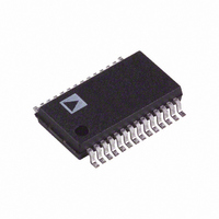
AD9851BRS Analog Devices Inc, AD9851BRS Datasheet - Page 7

AD9851BRS
Manufacturer Part Number
AD9851BRS
Description
Direct Digital Synthesizer 180MHz 1-DAC 10-Bit Parallel/Serial 28-Pin SSOP
Manufacturer
Analog Devices Inc
Datasheet
1.AD9851BRSZ.pdf
(24 pages)
Specifications of AD9851BRS
Resolution
10 Bit
Maximum Input Frequency
180 MHz
Tuning Word Width
32 Bit
Minimum Operating Supply Voltage
2.7 V
Typical Operating Supply Voltage
5 V
Maximum Operating Supply Voltage
5.25 V
Minimum Operating Temperature
-40 °C
Maximum Operating Temperature
85 °C
Rohs Status
RoHS non-compliant
Resolution (bits)
10 b
Master Fclk
180MHz
Tuning Word Width (bits)
32 b
Voltage - Supply
2.7 V ~ 5.25 V
Operating Temperature
-40°C ~ 85°C
Mounting Type
Surface Mount
Package / Case
28-SSOP
For Use With
AD9951/PCBZ - BOARD EVALUATION FOR AD9851
Lead Free Status / RoHS Status
Available stocks
Company
Part Number
Manufacturer
Quantity
Price
Part Number:
AD9851BRS
Manufacturer:
ADI/亚德诺
Quantity:
20 000
Company:
Part Number:
AD9851BRSZ
Manufacturer:
ADI41
Quantity:
377
TPC 7. Typical CMOS comparator p-p output jitter with
the AD9851 configured as a clock generator, DDS f
the AD9851 configured as a clock generator, DDS f
the AD9851 configured as a clock generator, DDS f
10.1 MHz, V
10.1 MHz, V
10.1 MHz, V = 5 V, system clock = 180 MHz, 70 MHz LPF .
Graph details the center portion of a rising edge with
scope in delayed trigger mode, 200 ps/div. Cursors show
208 ps p-p jitter.
TPC 8. Typical CMOS comparator p-p output jitter with the
AD9851 configured as a clock generator, DDS f
AD9851 configured as a clock generator, DDS f
AD9851 configured as a clock generator, DDS f
V
V
V = 5 V, system clock = 180 MHz, 70 MHz LPF. Graph details
the center portion of a rising edge with scope in delayed
trigger mode, 200 ps/div. Cursors show 204 ps p-p jitter.
REV. D
S
S
S
S
= 5 V, system clock = 180 MHz, 70 MHz LPF. Graph details
1
1
Tek Run 4.00GS/s
Tek Run 4.00GS/s
Ch1 200mV
Ch1 200mV
S
S
S
S
@ : 1.940ns
: 204ps
@ : 3.672ns
: 208ps
= 5 V, system clock = 180 MHz, 70 MHz LPF .
T
Sample
Sample
T
[
[
]
]
M 12.5ns Ch 1
D 200ps Runs After
M 12.5ns Ch 1
D 200ps Runs After
OUT
OUT
OUT
OUT
–200mV
–200mV
= 40.1 MHz,
= 40.1 MHz,
OUT
OUT
OUT
OUT
=
=
–7–
TPC 10. Output Phase Noise (5.2 MHz A
Multiplier Enabled, System Clock = 180 MHz, Reference
Clock = 30 MHz
TPC 9. Typical CMOS comparator p-p output
jitter with the AD9851 configured as a clock
generator, DDS f
generator, DDS f
generator, DDS f
clock = 180 MHz, 70 MHz LPF. Graph details
the center portion of a rising edge with scope
in delayed trigger mode, 200 ps/div. Cursors
show 280 ps p-p jitter.
1
–100
–115
–120
–125
–130
–135
–140
–145
Tek Run 4.00GS/s
100
Ch1 200mV
@ : 2.668ns
: 280ps
OUT
OUT
OUT
OUT
FREQUENCY OFFSET – Hz
Sample
1k
T
= 70.1 MHz, V
= 70.1 MHz, V
= 70.1 MHz, V
= 70.1 MHz, V = 5 V, system
[
]
M 12.5ns Ch 1
D 200ps Runs After
AD9851 PHASE NOISE
10k
S
S
S
S
OUT
OUT
OUT
= 5 V, system
), 6
), 6
AD9851
–200mV
REFCLK
100k


