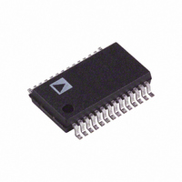
AD9851BRS Analog Devices Inc, AD9851BRS Datasheet - Page 16

AD9851BRS
Manufacturer Part Number
AD9851BRS
Description
Direct Digital Synthesizer 180MHz 1-DAC 10-Bit Parallel/Serial 28-Pin SSOP
Manufacturer
Analog Devices Inc
Datasheet
1.AD9851BRSZ.pdf
(24 pages)
Specifications of AD9851BRS
Resolution
10 Bit
Maximum Input Frequency
180 MHz
Tuning Word Width
32 Bit
Minimum Operating Supply Voltage
2.7 V
Typical Operating Supply Voltage
5 V
Maximum Operating Supply Voltage
5.25 V
Minimum Operating Temperature
-40 °C
Maximum Operating Temperature
85 °C
Rohs Status
RoHS non-compliant
Resolution (bits)
10 b
Master Fclk
180MHz
Tuning Word Width (bits)
32 b
Voltage - Supply
2.7 V ~ 5.25 V
Operating Temperature
-40°C ~ 85°C
Mounting Type
Surface Mount
Package / Case
28-SSOP
For Use With
AD9951/PCBZ - BOARD EVALUATION FOR AD9851
Lead Free Status / RoHS Status
Available stocks
Company
Part Number
Manufacturer
Quantity
Price
Part Number:
AD9851BRS
Manufacturer:
ADI/亚德诺
Quantity:
20 000
Company:
Part Number:
AD9851BRSZ
Manufacturer:
ADI41
Quantity:
377
*This bit is always Logic 0.
AD9851
Figure 19. Serial Load Frequency/Phase Update Sequence
W CLK
DATA
FQ UD
W0
W1
W2
W3
W4
W5
W6
W7
W8
W9
W10
W11
W12
W13
W14
W15
W16
W17
W18
W19
W20
W21
W22
W23
W24
W25
W26
W27
W28
W29
W30
W31
W32
W33
W34
W35
W36
W37
W38
W39
Table III. 40-Bit Serial Load Word Functional Assignment
W0
W1
Freq–b0 (LSB)
Freq–b1
Freq–b2
Freq–b3
Freq–b4
Freq–b5
Freq–b6
Freq–b7
Freq–b8
Freq–b9
Freq–b10
Freq–b11
Freq–b12
Freq–b13
Freq–b14
Freq–b15
Freq–b16
Freq–b17
Freq–b18
Freq–b19
Freq–b20
Freq–b21
Freq–b22
Freq–b23
Freq–b24
Freq–b25
Freq–b26
Freq–b27
Freq–b28
Freq–b29
Freq–b30
Freq–b31 (MSB)
6 REFCLK Multiplier Enable
Logic 0*
Power-Down
Phase–b0 (LSB)
Phase–b1
Phase–b2
Phase–b3
Phase–b4 (MSB)
40
40 W W CLK CYCLES
W2
CLK CYCLES
W3
W39
–16–
DATA (7) –
Figure 20 shows a normal 40-bit serial word load sequence with
W33 always set to Logic 0 and W34 set to Logic 1 or Logic 0
to control the power-down function. The logic states of the
remaining 38 bits are unimportant and are marked with an X,
indicating “don’t care” status. To power down, set W34 = 1. To
power up from a powered down state, change W34 to Logic 0.
Wake-up from power-down mode requires approximately 5 µs.
Note: The 40-bit input register of the AD9851 is fully program-
mable while in the power-down mode.
Figure 20. Serial Load Power-Down\Power-Up Sequence
W CLK
FQ UD
b. Comparator Output
a. DAC Output
IOUT
V
V
DD
Figure 21. I/O Equivalent Circuits
DD
IOUTB
W0 = X
DIGITAL
OUT
W33 = 0
40 W_CLK RISING EDGES
W34 = 1
OR 0
W35 = X
c. Comparator Input
DIGITAL
VINP/
VINN
d. Digital Input
W38 = X
IN
W39 = X
V
DD
REV. D
V
DD


