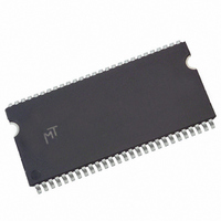
MT48LC4M16A2TG-75 IT:G TR Micron Technology Inc, MT48LC4M16A2TG-75 IT:G TR Datasheet - Page 35

MT48LC4M16A2TG-75 IT:G TR
Manufacturer Part Number
MT48LC4M16A2TG-75 IT:G TR
Description
DRAM Chip SDRAM 64M-Bit 4Mx16 3.3V 54-Pin TSOP-II T/R
Manufacturer
Micron Technology Inc
Type
SDRAMr
Datasheet
1.MT48LC4M16A2P-75G_TR.pdf
(72 pages)
Specifications of MT48LC4M16A2TG-75 IT:G TR
Package
54TSOP-II
Density
64 Mb
Address Bus Width
14 Bit
Operating Supply Voltage
3.3 V
Maximum Clock Rate
133 MHz
Maximum Random Access Time
6|5.4 ns
Operating Temperature
-40 to 85 °C
Format - Memory
RAM
Memory Type
SDRAM
Memory Size
64M (4M x 16)
Speed
133MHz
Interface
Parallel
Voltage - Supply
3 V ~ 3.6 V
Package / Case
54-TSOP II
Lead Free Status / RoHS Status
Contains lead / RoHS non-compliant
Other names
557-1090-2
Figure 26:
Clock Suspend
Burst Read/Single Write
PDF: 09005aef80725c0b/Source: 09005aef806fc13c
64MSDRAM_2.fm - Rev. N 12/08 EN
Power-Down
COMMAND
The clock suspend mode occurs when a column access/burst is in progress and CKE is
registered LOW. In the clock suspend mode, the internal clock is deactivated, “freezing”
the synchronous logic.
For each positive clock edge on which CKE is sampled LOW, the next internal positive
clock edge is suspended. Any command or data present on the input pins at the time of a
suspended internal clock edge is ignored; any data present on the DQ pins remains
driven; and burst counters are not incremented, as long as the clock is suspended. (See
examples in Figures 27 and 28 on page 36.)
Clock suspend mode is exited by registering CKE HIGH; the internal clock and related
operation will resume on the subsequent positive clock edge.
The burst read/single write mode is entered by programming the write burst mode bit
(M9) in the mode register to a logic 1. In this mode, all WRITE commands result in the
access of a single column location (burst of one), regardless of the programmed burst
length. READ commands access columns according to the programmed burst length
and sequence, just as in the normal mode of operation (M9 = 0).
CKE
CLK
All banks idle
Enter power-down mode.
t CKS
NOP
Input buffers gated off
35
(
(
(
(
)
(
)
)
)
)
(
(
(
(
)
(
)
)
)
)
Exit power-down mode.
Micron Technology, Inc., reserves the right to change products or specifications without notice.
> t CKS
NOP
64Mb: x4, x8, x16 SDRAM
DON’T CARE
©2000 Micron Technology, Inc. All rights reserved.
ACTIVE
t RCD
t RAS
t RC
Commands


