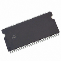
MT48LC8M16A2TG-75:G Micron Technology Inc, MT48LC8M16A2TG-75:G Datasheet - Page 27

MT48LC8M16A2TG-75:G
Manufacturer Part Number
MT48LC8M16A2TG-75:G
Description
DRAM Chip SDRAM 128M-Bit 8Mx16 3.3V 54-Pin TSOP-II Tray
Manufacturer
Micron Technology Inc
Type
SDRAMr
Datasheet
1.MT48LC8M16A2P-75G_TR.pdf
(74 pages)
Specifications of MT48LC8M16A2TG-75:G
Density
128 Mb
Maximum Clock Rate
133 MHz
Package
54TSOP-II
Address Bus Width
14 Bit
Operating Supply Voltage
3.3 V
Maximum Random Access Time
6|5.4 ns
Operating Temperature
0 to 70 °C
Format - Memory
RAM
Memory Type
SDRAM
Memory Size
128M (8Mx16)
Speed
133MHz
Interface
Parallel
Voltage - Supply
3 V ~ 3.6 V
Package / Case
54-TSOP II
Organization
8Mx16
Address Bus
14b
Access Time (max)
6/5.4ns
Operating Supply Voltage (typ)
3.3V
Package Type
TSOP-II
Operating Temp Range
0C to 70C
Operating Supply Voltage (max)
3.6V
Operating Supply Voltage (min)
3V
Supply Current
150mA
Pin Count
54
Mounting
Surface Mount
Operating Temperature Classification
Commercial
Lead Free Status / RoHS Status
Contains lead / RoHS non-compliant
Lead Free Status / RoHS Status
Not Compliant, Contains lead / RoHS non-compliant
Available stocks
Company
Part Number
Manufacturer
Quantity
Price
Company:
Part Number:
MT48LC8M16A2TG-75:G
Manufacturer:
MICRON
Quantity:
45
Part Number:
MT48LC8M16A2TG-75:G
Manufacturer:
MICRON
Quantity:
20 000
Figure 13:
PDF: 09005aef8091e66d/Source: 09005aef8091e625
128MSDRAM_2.fm - Rev. N 1/09 EN
Consecutive READ Bursts
Notes:
Data from any READ burst may be truncated with a subsequent READ command, and
data from a fixed-length READ burst may be immediately followed by data from a READ
command. In either case, a continuous flow of data can be maintained. The first data
element from the new burst either follows the last element of a completed burst or the
last desired data element of a longer burst that is being truncated. The new READ
command should be issued x cycles before the clock edge at which the last desired data
element is valid, where x = CL - 1.
This is shown in Figure 13 for L = 2 and CL = 3; data element n + 3 is either the last of a
burst of four or the last desired of a longer burst. The 128Mb SDRAM uses a pipelined
architecture and, therefore, does not require the 2n rule associated with a prefetch archi-
tecture. A READ command can be initiated on any clock cycle following a previous READ
command. Full-speed random read accesses can be performed to the same bank, as
shown in Figure 14 on page 28, or each subsequent READ may be performed to a
different bank.
COMMAND
COMMAND
1. Each READ command may be to any bank. DQM is LOW.
ADDRESS
ADDRESS
CLK
CLK
DQ
DQ
T0
T0
BANK,
COL n
BANK,
READ
COL n
READ
CL = 2
T1
T1
NOP
NOP
CL = 3
27
T2
T2
NOP
NOP
D
OUT
n
Micron Technology, Inc., reserves the right to change products or specifications without notice.
T3
T3
NOP
NOP
D
n + 1
D
n
OUT
OUT
TRANSITIONING DATA
T4
T4
BANK,
BANK,
READ
COL b
READ
COL b
X = 1 cycle
n + 1
n + 2
D
D
OUT
OUT
128Mb: x4, x8, x16 SDRAM
X = 2 cycles
T5
T5
NOP
NOP
n + 2
D
n + 3
D
OUT
OUT
©1999 Micron Technology, Inc. All rights reserved.
T6
T6
NOP
NOP
n + 3
D
D
OUT
OUT
b
DON’T CARE
Operations
T7
NOP
D
OUT
b


