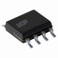
PBLS2002S,115 NXP Semiconductors, PBLS2002S,115 Datasheet - Page 13

PBLS2002S,115
Manufacturer Part Number
PBLS2002S,115
Description
LOADSWITCH PNP 20V 3A 8-SOIC
Manufacturer
NXP Semiconductors
Series
-r
Datasheet
1.PBLS2002S115.pdf
(16 pages)
Specifications of PBLS2002S,115
Package / Case
8-SOIC (3.9mm Width)
Transistor Type
1 NPN Pre-Biased, 1 PNP
Current - Collector (ic) (max)
100mA, 3A
Voltage - Collector Emitter Breakdown (max)
50V, 20V
Resistor - Base (r1) (ohms)
4.7K
Resistor - Emitter Base (r2) (ohms)
4.7K
Dc Current Gain (hfe) (min) @ Ic, Vce
30 @ 10mA, 5V / 150 @ 2A, 2V
Vce Saturation (max) @ Ib, Ic
150mV @ 500µA, 10mA / 355mV @ 300mA, 3A
Current - Collector Cutoff (max)
1µA, 100nA
Frequency - Transition
100MHz
Power - Max
1.5W
Mounting Type
Surface Mount
Configuration
Dual Dual Collector
Transistor Polarity
NPN/PNP
Typical Input Resistor
4.7 KOhms at NPN
Typical Resistor Ratio
1 at NPN
Mounting Style
SMD/SMT
Collector- Emitter Voltage Vceo Max
50 V at NPN, 20 V at PNP
Peak Dc Collector Current
100 mA at NPN, 3000 mA at PNP
Maximum Operating Temperature
+ 150 C
Minimum Operating Temperature
- 65 C
Lead Free Status / RoHS Status
Lead free / RoHS Compliant
Lead Free Status / RoHS Status
Lead free / RoHS Compliant, Lead free / RoHS Compliant
Other names
934060278115
PBLS2002S T/R
PBLS2002S T/R
PBLS2002S T/R
PBLS2002S T/R
NXP Semiconductors
11. Soldering
PBLS2002S_2
Product data sheet
Fig 20. Reflow soldering footprint SOT96-1 (SO8)
Fig 21. Wave soldering footprint SOT96-1 (SO8)
solder lands
occupied area
solder lands
occupied area
0.60 (6 )
placement accurracy
Rev. 02 — 24 August 2009
placement accuracy
solder resist
board direction
1.27 (6 )
0.3 (2 )
5.50
5.50
1.20 (2 )
0.60 (8 )
0.25
0.25
1.27 (6 )
1.30
4.00
1.30
4.00
Dimensions in mm
6.60
Dimensions in mm
enlarged solder land
6.60
7.00
7.00
20 V PNP BISS loadswitch
PBLS2002S
© NXP B.V. 2009. All rights reserved.
sot096-1_fw
sot096-1_fr
13 of 16


