AU5783D NXP Semiconductors, AU5783D Datasheet - Page 4
AU5783D
Manufacturer Part Number
AU5783D
Description
RF Transceiver J1850/VPW XCVR
Manufacturer
NXP Semiconductors
Datasheet
1.AU5783D-T.pdf
(14 pages)
Specifications of AU5783D
Number Of Receivers
1
Number Of Transmitters
1
Operating Supply Voltage
5.5 V to 16 V
Mounting Style
SMD/SMT
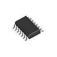
Package / Case
SOT-108
Lead Free Status / RoHS Status
Lead free / RoHS Compliant


Philips Semiconductors
PINNING
Pin configuration
Pin description
2001 Feb 15
R/F
GND
4X/LOOP
NSTB
TX
RX
N.C.
BAT
LWAKE
INH
LOAD
BUS
N.C.
GND
SYMBOL
J1850/VPW transceiver with supply control function
4X/LOOP
NSTB
GND
N.C.
R/F
RX
TX
PIN
10
12
13
14
11
1
2
3
4
5
6
7
8
9
Figure 2. Pin configuration
1
2
3
4
5
6
7
Rise/fall time control input; connect to ground
potential via a resistor
Ground
Tx mode control input; low: normal mode;
high: 4X mode; float: loopback
Network STandBy power control input; low:
transmit function disabled (low power modes);
high: transmit function enabled
Transmit data input; low: transmitter passive;
high: transmitter active
Receive data output; low: active bus condition
detected; high: otherwise
Not connected
Battery supply input, 12V nominal
Local wake-up input, edge sensitive
Activity indication flag (inhibit) output high side
driver; e.g., to control a voltage regulator.
Active high enables the regulator
Bus load in/output
Bus line transmit/receive input/output, active
high side driver
Not connected
Ground
AU5783
DESCRIPTION
SO14
10
9
8
14
13
12
11
SL01225
GND
N.C.
BUS
LOAD
INH
LWAKE
BAT
4
minimize ignition-off power consumption of an electronic control unit.
external devices, e.g., a voltage regulator. This condition will power-up
FUNCTIONAL DESCRIPTION
The AU5783 is an integrated line transceiver IC that interfaces an
SAE/J1850 protocol controller IC to the vehicle’s multiplex bus line.
It is primarily intended for automotive “Class B” multiplexing
applications in passenger cars using VPW (Variable Pulse Width)
modulated signals with a nominal transmission speed of 10.4 kbit/s.
The device provides transmit and receive capability as well as
protection to a J1850 electronic module.
A J1850 link controller feeds the transmit data stream to the
transceiver’s TX input. The AU5783 transceiver waveshapes the TX
data input signal so as to minimize electromagnetic emission. The
bus output signal features controlled rise & fall characteristic
including rounded shape. A resistance being connected to the R/F
control input sets the bus output slew rate.
The LOAD output is connected to the physical bus line via an
external load resistor R
ground potential being the default state, e.g., when no transmitter
outputs an active state. This output ensures the J1850 network will
not be affected by a potential loss of ground condition at an
individual electronic control unit.
The AU5783 includes a bus receiver with filter function to minimize
susceptibility against interference. The logic state of the J1850 bus
signal is indicated at the RX output being connected to the J1850
link controller.
The AU5783 also provides advanced low-power modes to help
The bus receiver function is kept alive in the low-power modes. If an
active state is being detected on the bus line this will be indicated
via the RX output. By default the AU5783 enters the low-power
standby mode when the mode control inputs NSTB and 4X/LOOP
are not driven. A 100 k pull down resistor is required on NSTB.
Ignition-off current draw can be reduced further by turning off the
voltage regulator being typically provided in an electronic control
unit. This is supported by the activity indication function of the
AU5783. In this application the activity indication flag INH will control
external devices such as a voltage regulator. To turn-off the INH flag
and thus the voltage regulator, the go to sleep command needs to
be applied to the Network Standby power control input,
e.g., NSTB = 0. The INH output is turned off after the sleep time-out
period thereby, reducing the power consumption of an electronic
control unit to an extremely low level.
The activity indication flag INH will be turned on again upon
detection of a remote wake-up condition (i.e. bus activity) or upon
detection of a local wake-up condition or a respective command
from the microcontroller. A local wake-up condition is detected
when an edge occurs at the wake-up input LWAKE. The INH flag
will also be turned on upon detection of a high input level at the
mode control input NSTB. Activation of the INH output enables
logic devices, e.g., a microcontroller in order to perform appropriate
action, e.g., activation of the AU5783 and the J1850 network.
The AU5783 contain a power on reset (POR) circuit, which is active
at low voltages. This circuit insures that if the control input NSTB is
at 0 V or floating during power up, the device will be forced into the
standby mode by the time the battery voltage rises to 4.4 V. This will
also insure that the INH pin is in the high state to turn on the local
voltage regulator. If there is a dip going below 4.4 V in battery
voltage while in the sleep mode, the device may return to the
ld
. The load resistor pulls the bus line to
Preliminary specification
AU5783
Related parts for AU5783D
Image
Part Number
Description
Manufacturer
Datasheet
Request
R

Part Number:
Description:
NXP Semiconductors designed the LPC2420/2460 microcontroller around a 16-bit/32-bitARM7TDMI-S CPU core with real-time debug interfaces that include both JTAG andembedded trace
Manufacturer:
NXP Semiconductors
Datasheet:

Part Number:
Description:
NXP Semiconductors designed the LPC2458 microcontroller around a 16-bit/32-bitARM7TDMI-S CPU core with real-time debug interfaces that include both JTAG andembedded trace
Manufacturer:
NXP Semiconductors
Datasheet:
Part Number:
Description:
NXP Semiconductors designed the LPC2468 microcontroller around a 16-bit/32-bitARM7TDMI-S CPU core with real-time debug interfaces that include both JTAG andembedded trace
Manufacturer:
NXP Semiconductors
Datasheet:
Part Number:
Description:
NXP Semiconductors designed the LPC2470 microcontroller, powered by theARM7TDMI-S core, to be a highly integrated microcontroller for a wide range ofapplications that require advanced communications and high quality graphic displays
Manufacturer:
NXP Semiconductors
Datasheet:
Part Number:
Description:
NXP Semiconductors designed the LPC2478 microcontroller, powered by theARM7TDMI-S core, to be a highly integrated microcontroller for a wide range ofapplications that require advanced communications and high quality graphic displays
Manufacturer:
NXP Semiconductors
Datasheet:
Part Number:
Description:
The Philips Semiconductors XA (eXtended Architecture) family of 16-bit single-chip microcontrollers is powerful enough to easily handle the requirements of high performance embedded applications, yet inexpensive enough to compete in the market for hi
Manufacturer:
NXP Semiconductors
Datasheet:
Part Number:
Description:
The XA-S3 device is a member of Philips Semiconductors? XA(eXtended Architecture) family of high performance 16-bitsingle-chip microcontrollers
Manufacturer:
NXP Semiconductors
Datasheet:

Part Number:
Description:
The NXP BlueStreak LH75401/LH75411 family consists of two low-cost 16/32-bit System-on-Chip (SoC) devices
Manufacturer:
NXP Semiconductors
Datasheet:
Part Number:
Description:
The NXP LPC3130/3131 combine an 180 MHz ARM926EJ-S CPU core, high-speed USB2
Manufacturer:
NXP Semiconductors
Datasheet:
Part Number:
Description:
The NXP LPC3141 combine a 270 MHz ARM926EJ-S CPU core, High-speed USB 2
Manufacturer:
NXP Semiconductors
Part Number:
Description:
The NXP LPC3143 combine a 270 MHz ARM926EJ-S CPU core, High-speed USB 2
Manufacturer:
NXP Semiconductors

Part Number:
Description:
The NXP LPC3152 combines an 180 MHz ARM926EJ-S CPU core, High-speed USB 2
Manufacturer:
NXP Semiconductors
Part Number:
Description:
The NXP LPC3154 combines an 180 MHz ARM926EJ-S CPU core, High-speed USB 2
Manufacturer:
NXP Semiconductors

Part Number:
Description:
Standard level N-channel enhancement mode Field-Effect Transistor (FET) in a plastic package using NXP High-Performance Automotive (HPA) TrenchMOS technology
Manufacturer:
NXP Semiconductors
Datasheet: