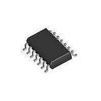
AU5783D NXP Semiconductors, AU5783D Datasheet - Page 9

AU5783D
Manufacturer Part Number
AU5783D
Description
RF Transceiver J1850/VPW XCVR
Manufacturer
NXP Semiconductors
Datasheet
1.AU5783D-T.pdf
(14 pages)
Specifications of AU5783D
Number Of Receivers
1
Number Of Transmitters
1
Operating Supply Voltage
5.5 V to 16 V
Mounting Style
SMD/SMT
Package / Case
SOT-108
Lead Free Status / RoHS Status
Lead free / RoHS Compliant
1. TX = 0 V; NSTB = 0 V; 7 V < V
2. This parameter is characterized but not subject to production test.
3. For V
Philips Semiconductors
NOTES:
4. For 3-State devices driving the 4X/LOOP Pin, the leakage in the 3-State output must be below the specified input current to ensure the pin is
2001 Feb 15
Pin BUS
Pin LOAD
J1850/VPW transceiver with supply control function
SYMBOL
V
V
V
–I
–I
–I
–I
–I
–I
–I
V
V
V
V
V
V
V
V
V
V
V
For 16 V < V
to be less than 2 minutes.
biased in the center state to provide the loop back function. For 3-State devices driving the 4X/LOOP pin, the leakage in the 3-State output
must be below the specified input current to insure the pin is biased in the center state to provide the loop back function. If the leakage
current of the microcontroller is too high, then an alternate approach is to connect a resistor voltage divider between the V
the microcontroller’s supply to provide approximately 1.45 V bias on the 4X/LOOP pin.
BOh_n
BOh_h
BOhl
Bih
Bil
Bhy
Bih_l
BiL_L
Bih_s
Bil_s
Bih_sl
Bil_sl
ld
ldoff
BO.LIM
BO.LK1
BO.LK0
BO.LK5
BO.LKLB0
BO.LKLB5
LOG
BAT
,
< 8.3 V the bus output voltage is limited by the supply voltage.
,
BAT
BUS output high voltage in normal mode
BUS output high voltage in high speed
mode
BUS voltage; low battery
BUS short circuit current
BUS leakage current; passive state
BUS current with loss of battery
BUS leakage current; loop back mode
BUS leakage current at loss of ground
BUS input high voltage
BUS input low voltage
BUS input hysteresis
BUS input high voltage at low battery
BUS input low voltage at low battery
BUS input high voltage in standby and
sleep mode
BUS input low voltage in standby
and sleep mode
BUS input high voltage in standby and
sleep mode at low battery
BUS input low voltage in standby and
sleep mode at low battery
Load output voltage
Load output voltage unpowered
< 27 V the load is limited by the package power dissipation ratings. The duration of the latter condition is recommended
PARAMETER
BAT
< 13 V; T
j
< 125 C; –1 V < V
TX = 5 V, 4X/LOOP = 0 V;
8 V < V
250
TX = 5 V, 4X/LOOP = 5 V;
8 V < V
250
TX = 5 V; Note 3
5.5 V<V
250
TX = 5 V; V
TX = 0 V; 0 V < V
–2 V < V
V
TX = 0 V or 5 V; 0 V<V
–2 V < V
0 V < V
5.8 V < V
4X/LOOP = 5 V and
4X/LOOP = 0 V
4X/LOOP = 5 V or
4X/LOOP = 0 V
4X/LOOP = 5 V and
4X/LOOP = 0 V
5.5 V < V
4X/LOOP = 5 V and
4X/LOOP = 0 V
5.5 V < V
4X/LOOP = 5 V and
4X/LOOP = 0 V
NSTB = 0 V,
4X/LOOP = 5 V and
4X/LOOP = 0 V,
6 V < V
NSTB = 0 V,
4X/LOOP = 5 V and
4X/LOOP = 0 V,
6 V < V
NSTB = 0 V,
4X/LOOP = 5 V and
4X/LOOP = 0 V ,
4.5 V < V
NSTB = 0 V,
4X/LOOP = 5 V and
4X/LOOP = 0 V ,
4.5 V < V
Il
I
ld
d
BAT
= 2 mA
= 6 mA, V
BUS
< 2 V; –2 V < V
< R
< R
< R
BAT
BAT
BAT
BAT
BAT
BAT
BUS
BUS
BAT
BAT
BAT
BAT
BAT
9
< 1 V; LWAKE connected to BAT via 10 k ; INH not connected.
CONDITIONS
L
L
L
< 16 V
< 16 V
BUS
< 16 V; see test circuit
< 16 V
< 16 V
< 1.6 k ; Note 3
< 1.6 k ; Note 3
< 1.6 k
< 8 V;
BAT
< 16 V,
< 5.8 V,
< 7 V,
< 6 V
< 6 V
< +9 V
< +9 V
= –2 V
= 0 V
BAT
< 16 V;
BUS
BAT
< +9 V
<16 V;
6.7
6.7
V
30
–100
–100
–100
–20
4.2
0.1
V
1.6 V
4.2
1
2.4)
/
BAT
BAT
2
MIN.
(V
–1.3
–
BAT
+
TYP.
Preliminary specification
8.0
9.0
V
100
+100
+100
+100
+100
3.4
0.5
V
3.6 V
2.2
1
1.6)
0.2
1
/
BAT
BAT
2
CC
MAX.
(V
AU5783
and ground of
BAT
–
–
V
V
V
mA
V
V
V
V
V
V
V
V
V
V
V
UNIT
A
A
A
A


