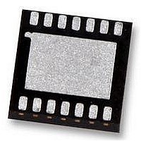
LMP91000SDE National Semiconductor, LMP91000SDE Datasheet - Page 13

LMP91000SDE
Manufacturer Part Number
LMP91000SDE
Description
AFE, SENSOR, 14LLP
Manufacturer
National Semiconductor
Datasheet
1.LMP91000SDENOPB.pdf
(24 pages)
Specifications of LMP91000SDE
Brief Features
Programmable Cell Bias Voltage, Low Bias Voltage Drift, I2C Compatible Digital Interface
Supply Voltage Range
2.7V To 5.25V
Operating Temperature Range
-40°C To +85°C
Digital Ic Case Style
LLP
Ic Function
Programmable Analogue Front End (AFE)
Rohs Compliant
Yes
Lead Free Status / RoHS Status
Lead free / RoHS Compliant
Available stocks
Company
Part Number
Manufacturer
Quantity
Price
Part Number:
LMP91000SDE/NOPB
Manufacturer:
TI/德州仪器
Quantity:
20 000
WRITE AND READ OPERATION
In order to start any read or write operation with the
LMP91000, MENB needs to be set low during the whole com-
munication. Then the master generates a start condition by
driving SDA from high to low while SCL is high. The start con-
dition is always followed by a 7-bit slave address and a Read/
Write bit. After these 8 bits have been transmitted by the mas-
ter, SDA is released by the master and the LMP91000 either
ACKs or NACKs the address. If the slave address matches,
the LMP91000 ACKs the master. If the address doesn't
match, the LMP91000 NACKs the master. For a write opera-
tion, the master follows the ACK by sending the 8-bit register
address pointer. Then the LMP91000 ACKs the transfer by
driving SDA low. Next, the master sends the 8-bit data to the
LMP91000. Then the LMP91000 ACKs the transfer by driving
FIGURE 3. READ and WRITE transaction
(a) Register write transaction
(c) Register read transaction
(b) Pointer set transaction
13
SDA low. At this point the master should generate a stop con-
dition and optionally set the MENB at logic high level (refer
to
A read operation requires the LMP91000 address pointer to
be set first, also in this case the master needs setting at low
logic level the MENB, then the master needs to write to the
device and set the address pointer before reading from the
desired register. This type of read requires a start, the slave
address, a write bit, the address pointer, a Repeated Start (if
appropriate), the slave address, and a read bit (refer to
Figure
the 8-bit data of the register.
When just one LMP91000 is present on the I
can be tied to ground (low logic level).
Figure
3). Following this sequence, the LMP91000 sends out
3).
30132572
2
C bus the MENB
30132571
30132570
www.national.com


