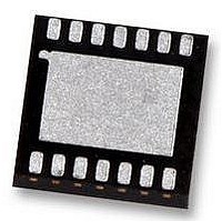
LMP91000SDE National Semiconductor, LMP91000SDE Datasheet - Page 14

LMP91000SDE
Manufacturer Part Number
LMP91000SDE
Description
AFE, SENSOR, 14LLP
Manufacturer
National Semiconductor
Datasheet
1.LMP91000SDENOPB.pdf
(24 pages)
Specifications of LMP91000SDE
Brief Features
Programmable Cell Bias Voltage, Low Bias Voltage Drift, I2C Compatible Digital Interface
Supply Voltage Range
2.7V To 5.25V
Operating Temperature Range
-40°C To +85°C
Digital Ic Case Style
LLP
Ic Function
Programmable Analogue Front End (AFE)
Rohs Compliant
Yes
Lead Free Status / RoHS Status
Lead free / RoHS Compliant
Available stocks
Company
Part Number
Manufacturer
Quantity
Price
Part Number:
LMP91000SDE/NOPB
Manufacturer:
TI/德州仪器
Quantity:
20 000
www.national.com
TIMEOUT FEATURE
The timeout is a safety feature to avoid bus lockup situation.
If SCL is stuck low for a time exceeding t_timeout, the
LMP91000 will automatically reset its I
the case the LMP91000 hangs the SDA for a time exceeding
REGISTERS
The registers are used to configure the LMP91000.
If writing to a reserved bit, user must write only 0. Readback value is unspecified and should be discarded.
STATUS -- Status Register (address 0x00)
The status bit is an indication of the LMP91000's power-on status. If its readback is “0”, the LMP91000 is not ready to accept other
I
LOCK -- Protection Register (address 0x01)
The lock bit enables and disables the writing of the TIACN and the REFCN registers. In order to change the content of the TIACN
and the REFCN registers the lock bit needs to be set to “0”.
2
C commands.
0x02 through 0x09
0x13 through 0xFF
[7:1]
[7:1]
Bit
Bit
0
0
Address
0x00
0x01
0x10
0x11
0x12
RESERVED
RESERVED
STATUS
Name
Name
LOCK
RESERVED
RESERVED
MODECN
STATUS
REFCN
TIACN
Name
LOCK
2
C interface. Also, in
Status of Device
0 Not Ready (default)
1 Ready
Write protection
0 Registers 0x10, 0x11 in write mode
1 Registers 0x10, 0x11 in read only mode (default)
Power on default
Register map
14
0x1C
0x00
0x01
0x00
0x00
t_timeout, the LMP91000’s I
the SDA line will be released. Since the SDA is an open-drain
with an external resistor pull-up, this also avoids high power
consumption when LMP91000 is driving the bus and the SCL
is stopped.
Read only
Function
Function
Access
R/W
R/W
R/W
R/W
2
C interface will be reset so that
Lockable?
N
N
N
Y
Y


