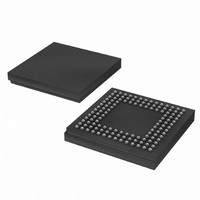
XC3S500E-4CPG132C Xilinx Inc, XC3S500E-4CPG132C Datasheet - Page 118

XC3S500E-4CPG132C
Manufacturer Part Number
XC3S500E-4CPG132C
Description
FPGA Spartan®-3E Family 500K Gates 10476 Cells 572MHz 90nm (CMOS) Technology 1.2V 132-Pin CSBGA
Manufacturer
Xilinx Inc
Series
Spartan™-3Er
Datasheet
1.XC3S100E-4VQG100C.pdf
(233 pages)
Specifications of XC3S500E-4CPG132C
Package
132CSBGA
Family Name
Spartan®-3E
Device Logic Cells
10476
Device Logic Units
1164
Device System Gates
500000
Number Of Registers
9312
Maximum Internal Frequency
572 MHz
Typical Operating Supply Voltage
1.2 V
Maximum Number Of User I/os
92
Ram Bits
368640
Number Of Logic Elements/cells
10476
Number Of Labs/clbs
1164
Total Ram Bits
368640
Number Of I /o
92
Number Of Gates
500000
Voltage - Supply
1.14 V ~ 1.26 V
Mounting Type
Surface Mount
Operating Temperature
0°C ~ 85°C
Package / Case
132-TFBGA, CSPBGA
Lead Free Status / RoHS Status
Lead free / RoHS Compliant
For Use With
122-1536 - KIT STARTER SPARTAN-3E
Lead Free Status / RoHS Status
Lead free / RoHS Compliant
Other names
122-1484
Available stocks
Company
Part Number
Manufacturer
Quantity
Price
Company:
Part Number:
XC3S500E-4CPG132C
Manufacturer:
Xilinx Inc
Quantity:
10 000
Part Number:
XC3S500E-4CPG132C
Manufacturer:
XILINX/赛灵思
Quantity:
20 000
- Current page: 118 of 233
- Download datasheet (6Mb)
DC and Switching Characteristics
Power Supply Specifications
Table 74: Supply Voltage Thresholds for Power-On Reset
Table 75: Supply Voltage Ramp Rate
Table 76: Supply Voltage Levels Necessary for Preserving RAM Contents
118
Notes:
1.
2.
Notes:
1.
2.
Notes:
1.
V
SPI Flash, parallel NOR Flash, microcontroller) might have specific requirements. Check the data sheet for the attached configuration
source. In Step 0 devices using the HSWAP internal pull-up, V
To ensure successful power-on, V
no dips at any point.
V
SPI Flash, parallel NOR Flash, microcontroller) might have specific requirements. Check the data sheet for the attached configuration
source. In Step 0 devices using the HSWAP internal pull-up, V
To ensure successful power-on, V
no dips at any point.
Symbol
RAM contents include configuration data.
V
V
CCINT
CCINT
DRAUX
V
V
DRINT
V
Symbol
V
Symbol
V
V
CCAUXR
CCAUXT
CCINTR
CCINTT
CCO2R
CCO2T
, V
, V
CCAUX
CCAUX
, and V
, and V
V
V
CCINT
CCAUX
Threshold for the V
Threshold for the V
Threshold for the V
Ramp rate from GND to valid V
Ramp rate from GND to valid V
Ramp rate from GND to valid V
CCO
CCO
level required to retain RAM data
level required to retain RAM data
supplies to the FPGA can be applied in any order. However, the FPGA’s configuration source (Platform Flash,
supplies to the FPGA can be applied in any order. However, the FPGA’s configuration source (Platform Flash,
CCINT
CCINT
, V
, V
CCO
CCO
CCINT
CCAUX
CCO
Bank 2, and V
Bank 2, and V
Description
Description
Bank 2 supply
supply
supply
Description
www.xilinx.com
CCINT
CCAUX
CCO
CCAUX
CCAUX
CCINT
CCINT
Bank 2 supply level
supply level
supplies must rise through their respective threshold-voltage ranges with
supplies must rise through their respective threshold-voltage ranges with
supply level
must be applied before V
must be applied before V
CCAUX
CCAUX
Min
Min
0.4
0.8
0.4
0.2
0.2
0.2
.
.
DS312-3 (v3.8) August 26, 2009
Max
Max
1.0
2.0
1.0
50
50
50
Product Specification
Min
1.0
2.0
Units
Units
Units
ms
ms
ms
V
V
V
V
V
R
Related parts for XC3S500E-4CPG132C
Image
Part Number
Description
Manufacturer
Datasheet
Request
R

Part Number:
Description:
IC SPARTAN-3E FPGA 500K 320FBGA
Manufacturer:
Xilinx Inc
Datasheet:

Part Number:
Description:
IC FPGA SPARTAN-3E 500K 208-PQFP
Manufacturer:
Xilinx Inc
Datasheet:

Part Number:
Description:
IC FPGA SPARTAN-3E 500K 132CSBGA
Manufacturer:
Xilinx Inc
Datasheet:

Part Number:
Description:
IC FPGA SPARTAN-3E 500K 256FTBGA
Manufacturer:
Xilinx Inc
Datasheet:

Part Number:
Description:
IC FPGA SPARTAN-3E 500K 256FTBGA
Manufacturer:
Xilinx Inc
Datasheet:

Part Number:
Description:
IC FPGA SPARTAN-3E 500K 320-FBGA
Manufacturer:
Xilinx Inc
Datasheet:

Part Number:
Description:
IC FPGA SPARTAN 3E 320FBGA
Manufacturer:
Xilinx Inc
Datasheet:

Part Number:
Description:
FPGA Spartan®-3E Family 500K Gates 10476 Cells 572MHz 90nm (CMOS) Technology 1.2V 256-Pin FTBGA
Manufacturer:
Xilinx Inc
Datasheet:

Part Number:
Description:
FPGA Spartan®-3E Family 500K Gates 10476 Cells 572MHz 90nm (CMOS) Technology 1.2V 208-Pin PQFP
Manufacturer:
Xilinx Inc
Datasheet:

Part Number:
Description:
FPGA Spartan®-3E Family 500K Gates 10476 Cells 572MHz 90nm (CMOS) Technology 1.2V 208-Pin PQFP
Manufacturer:
Xilinx Inc
Datasheet:

Part Number:
Description:
FPGA Spartan®-3E Family 500K Gates 10476 Cells 572MHz 90nm (CMOS) Technology 1.2V 256-Pin FTBGA
Manufacturer:
Xilinx Inc
Datasheet:

Part Number:
Description:
FPGA Spartan-3E Family 500K Gates 10476 Cells 572MHz 90nm (CMOS) Technology 1.2V 320-Pin FBGA
Manufacturer:
Xilinx Inc
Datasheet:

Part Number:
Description:
IC FPGA SPARTAN-3E 500K 100-VQFP
Manufacturer:
Xilinx Inc
Datasheet:

Part Number:
Description:
IC FPGA SPARTAN-3E 500K 132CSBGA
Manufacturer:
Xilinx Inc
Datasheet:

Part Number:
Description:
IC FPGA SPARTAN-3E 500K 320-FBGA
Manufacturer:
Xilinx Inc
Datasheet:


