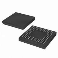
XC3S500E-4CPG132C Xilinx Inc, XC3S500E-4CPG132C Datasheet - Page 153

XC3S500E-4CPG132C
Manufacturer Part Number
XC3S500E-4CPG132C
Description
FPGA Spartan®-3E Family 500K Gates 10476 Cells 572MHz 90nm (CMOS) Technology 1.2V 132-Pin CSBGA
Manufacturer
Xilinx Inc
Series
Spartan™-3Er
Datasheet
1.XC3S100E-4VQG100C.pdf
(233 pages)
Specifications of XC3S500E-4CPG132C
Package
132CSBGA
Family Name
Spartan®-3E
Device Logic Cells
10476
Device Logic Units
1164
Device System Gates
500000
Number Of Registers
9312
Maximum Internal Frequency
572 MHz
Typical Operating Supply Voltage
1.2 V
Maximum Number Of User I/os
92
Ram Bits
368640
Number Of Logic Elements/cells
10476
Number Of Labs/clbs
1164
Total Ram Bits
368640
Number Of I /o
92
Number Of Gates
500000
Voltage - Supply
1.14 V ~ 1.26 V
Mounting Type
Surface Mount
Operating Temperature
0°C ~ 85°C
Package / Case
132-TFBGA, CSPBGA
Lead Free Status / RoHS Status
Lead free / RoHS Compliant
For Use With
122-1536 - KIT STARTER SPARTAN-3E
Lead Free Status / RoHS Status
Lead free / RoHS Compliant
Other names
122-1484
Available stocks
Company
Part Number
Manufacturer
Quantity
Price
Company:
Part Number:
XC3S500E-4CPG132C
Manufacturer:
Xilinx Inc
Quantity:
10 000
Part Number:
XC3S500E-4CPG132C
Manufacturer:
XILINX/赛灵思
Quantity:
20 000
- Current page: 153 of 233
- Download datasheet (6Mb)
Master Serial and Slave Serial Mode Timing
Table 116: Timing for the Master Serial and Slave Serial Configuration Modes
DS312-3 (v3.8) August 26, 2009
Product Specification
(Input/Output)
Notes:
1.
2.
(Open-Drain)
Clock-to-Output Times
T
Setup Times
T
Hold Times
T
Clock Timing
T
T
F
Symbol
CCO
DCC
CCD
CCH
CCL
CCSER
PROG_B
The numbers in this table are based on the operating conditions set forth in
For serial configuration with a daisy-chain of multiple FPGAs, the maximum limit is 25 MHz.
(Output)
INIT_B
(Input)
(Input)
DOUT
CCLK
DIN
R
The time from the falling transition on the CCLK pin to data
appearing at the DOUT pin
The time from the setup of data at the DIN pin to the active edge of
the CCLK pin
The time from the active edge of the CCLK pin to the point when
data is last held at the DIN pin
High pulse width at the CCLK input pin
Low pulse width at the CCLK input pin
Frequency of the clock signal at
the CCLK input pin
Figure 75: Waveforms for Master Serial and Slave Serial Configuration
Description
T
DCC
Bit 0
No bitstream compression
With bitstream compression
www.xilinx.com
T
CCD
Bit 1
Table
77.
T
T
Master
Master
Master
Slave/
MCCL
Slave
Slave
Slave
SCCL
Both
Both
Both
DC and Switching Characteristics
Bit n
1/F
CCSER
T
CCO
Bit n-64
All Speed Grades
Bit n+1
11.0
Min
1.5
T
T
0
0
0
MCCH
SCCH
See
See
See
See
Bit n-63
Table 114
Table 115
Table 114
Table 115
66
Max
10.0
20
-
-
(2)
DS312-3_05_103105
Units
MHz
MHz
ns
ns
ns
153
Related parts for XC3S500E-4CPG132C
Image
Part Number
Description
Manufacturer
Datasheet
Request
R

Part Number:
Description:
IC SPARTAN-3E FPGA 500K 320FBGA
Manufacturer:
Xilinx Inc
Datasheet:

Part Number:
Description:
IC FPGA SPARTAN-3E 500K 208-PQFP
Manufacturer:
Xilinx Inc
Datasheet:

Part Number:
Description:
IC FPGA SPARTAN-3E 500K 132CSBGA
Manufacturer:
Xilinx Inc
Datasheet:

Part Number:
Description:
IC FPGA SPARTAN-3E 500K 256FTBGA
Manufacturer:
Xilinx Inc
Datasheet:

Part Number:
Description:
IC FPGA SPARTAN-3E 500K 256FTBGA
Manufacturer:
Xilinx Inc
Datasheet:

Part Number:
Description:
IC FPGA SPARTAN-3E 500K 320-FBGA
Manufacturer:
Xilinx Inc
Datasheet:

Part Number:
Description:
IC FPGA SPARTAN 3E 320FBGA
Manufacturer:
Xilinx Inc
Datasheet:

Part Number:
Description:
FPGA Spartan®-3E Family 500K Gates 10476 Cells 572MHz 90nm (CMOS) Technology 1.2V 256-Pin FTBGA
Manufacturer:
Xilinx Inc
Datasheet:

Part Number:
Description:
FPGA Spartan®-3E Family 500K Gates 10476 Cells 572MHz 90nm (CMOS) Technology 1.2V 208-Pin PQFP
Manufacturer:
Xilinx Inc
Datasheet:

Part Number:
Description:
FPGA Spartan®-3E Family 500K Gates 10476 Cells 572MHz 90nm (CMOS) Technology 1.2V 208-Pin PQFP
Manufacturer:
Xilinx Inc
Datasheet:

Part Number:
Description:
FPGA Spartan®-3E Family 500K Gates 10476 Cells 572MHz 90nm (CMOS) Technology 1.2V 256-Pin FTBGA
Manufacturer:
Xilinx Inc
Datasheet:

Part Number:
Description:
FPGA Spartan-3E Family 500K Gates 10476 Cells 572MHz 90nm (CMOS) Technology 1.2V 320-Pin FBGA
Manufacturer:
Xilinx Inc
Datasheet:

Part Number:
Description:
IC FPGA SPARTAN-3E 500K 100-VQFP
Manufacturer:
Xilinx Inc
Datasheet:

Part Number:
Description:
IC FPGA SPARTAN-3E 500K 132CSBGA
Manufacturer:
Xilinx Inc
Datasheet:

Part Number:
Description:
IC FPGA SPARTAN-3E 500K 320-FBGA
Manufacturer:
Xilinx Inc
Datasheet:


