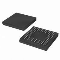
XC3S500E-4CPG132C Xilinx Inc, XC3S500E-4CPG132C Datasheet - Page 72

XC3S500E-4CPG132C
Manufacturer Part Number
XC3S500E-4CPG132C
Description
FPGA Spartan®-3E Family 500K Gates 10476 Cells 572MHz 90nm (CMOS) Technology 1.2V 132-Pin CSBGA
Manufacturer
Xilinx Inc
Series
Spartan™-3Er
Datasheet
1.XC3S100E-4VQG100C.pdf
(233 pages)
Specifications of XC3S500E-4CPG132C
Package
132CSBGA
Family Name
Spartan®-3E
Device Logic Cells
10476
Device Logic Units
1164
Device System Gates
500000
Number Of Registers
9312
Maximum Internal Frequency
572 MHz
Typical Operating Supply Voltage
1.2 V
Maximum Number Of User I/os
92
Ram Bits
368640
Number Of Logic Elements/cells
10476
Number Of Labs/clbs
1164
Total Ram Bits
368640
Number Of I /o
92
Number Of Gates
500000
Voltage - Supply
1.14 V ~ 1.26 V
Mounting Type
Surface Mount
Operating Temperature
0°C ~ 85°C
Package / Case
132-TFBGA, CSPBGA
Lead Free Status / RoHS Status
Lead free / RoHS Compliant
For Use With
122-1536 - KIT STARTER SPARTAN-3E
Lead Free Status / RoHS Status
Lead free / RoHS Compliant
Other names
122-1484
Available stocks
Company
Part Number
Manufacturer
Quantity
Price
Company:
Part Number:
XC3S500E-4CPG132C
Manufacturer:
Xilinx Inc
Quantity:
10 000
Part Number:
XC3S500E-4CPG132C
Manufacturer:
XILINX/赛灵思
Quantity:
20 000
- Current page: 72 of 233
- Download datasheet (6Mb)
Functional Description
Master Serial Mode
For additional information, refer to the Master Serial Mode
chapter in UG332.
In Master Serial mode (M[2:0] = <0:0:0>), the Spartan-3E
FPGA configures itself from an attached Xilinx Platform
All mode select pins, M[2:0], must be Low when sampled,
when the FPGA’s INIT_B output goes High. After configura-
tion, when the FPGA’s DONE output goes High, the mode
select pins are available as full-featured user-I/O pins.
enable pull-up resistors on all user-I/O pins during configu-
ration or High to disable the pull-up resistors. The HSWAP
control must remain at a constant logic level throughout
72
P
Recommend
Similarly, the FPGA’s HSWAP pin must be Low to
open-drain
PROG_B
driver
TMS
TDO
TCK
TDI
+2.5V
JTAG
Serial Master
Mode
‘0’
‘0’
‘0’
P
Figure 51: Master Serial Mode using Platform Flash PROM
HSWAP
M2
M1
M0
TDI
TMS
TCK
PROG_B
Spartan-3E
FPGA
VCCINT
+1.2V
GND
VCCAUX
VCCO_0
VCCO_2
INIT_B
DONE
DOUT
CCLK
TDO
DIN
www.xilinx.com
VCCO_0
+2.5V
V
Flash PROM, as illustrated in
plies the CCLK output clock from its internal oscillator to the
attached Platform Flash PROM. In response, the Platform
Flash PROM supplies bit-serial data to the FPGA’s DIN
input, and the FPGA accepts this data on each rising CCLK
edge.
FPGA configuration. After configuration, when the FPGA’s
DONE output goes High, the HSWAP pin is available as
full-featured user-I/O pin and is powered by the VCCO_0
supply.
The FPGA's DOUT pin is used in daisy-chain applications,
described later. In a single-FPGA application, the FPGA’s
DOUT pin is not used but is actively driving during the con-
figuration process.
+2.5V
V
D0
CLK
OE/RESET
CE
CF
TDI
TMS
TCK
Platform Flash
XCFxxS = +3.3V
XCFxxP = +1.8V
XCFxx
VCCINT
GND
DS312-2 (v3.8) August 26, 2009
Figure
VCCO
VCCJ
Product Specification
51. The FPGA sup-
CEO
TDO
DS312-2_44_082009
+2.5V
V
R
Related parts for XC3S500E-4CPG132C
Image
Part Number
Description
Manufacturer
Datasheet
Request
R

Part Number:
Description:
IC SPARTAN-3E FPGA 500K 320FBGA
Manufacturer:
Xilinx Inc
Datasheet:

Part Number:
Description:
IC FPGA SPARTAN-3E 500K 208-PQFP
Manufacturer:
Xilinx Inc
Datasheet:

Part Number:
Description:
IC FPGA SPARTAN-3E 500K 132CSBGA
Manufacturer:
Xilinx Inc
Datasheet:

Part Number:
Description:
IC FPGA SPARTAN-3E 500K 256FTBGA
Manufacturer:
Xilinx Inc
Datasheet:

Part Number:
Description:
IC FPGA SPARTAN-3E 500K 256FTBGA
Manufacturer:
Xilinx Inc
Datasheet:

Part Number:
Description:
IC FPGA SPARTAN-3E 500K 320-FBGA
Manufacturer:
Xilinx Inc
Datasheet:

Part Number:
Description:
IC FPGA SPARTAN 3E 320FBGA
Manufacturer:
Xilinx Inc
Datasheet:

Part Number:
Description:
FPGA Spartan®-3E Family 500K Gates 10476 Cells 572MHz 90nm (CMOS) Technology 1.2V 256-Pin FTBGA
Manufacturer:
Xilinx Inc
Datasheet:

Part Number:
Description:
FPGA Spartan®-3E Family 500K Gates 10476 Cells 572MHz 90nm (CMOS) Technology 1.2V 208-Pin PQFP
Manufacturer:
Xilinx Inc
Datasheet:

Part Number:
Description:
FPGA Spartan®-3E Family 500K Gates 10476 Cells 572MHz 90nm (CMOS) Technology 1.2V 208-Pin PQFP
Manufacturer:
Xilinx Inc
Datasheet:

Part Number:
Description:
FPGA Spartan®-3E Family 500K Gates 10476 Cells 572MHz 90nm (CMOS) Technology 1.2V 256-Pin FTBGA
Manufacturer:
Xilinx Inc
Datasheet:

Part Number:
Description:
FPGA Spartan-3E Family 500K Gates 10476 Cells 572MHz 90nm (CMOS) Technology 1.2V 320-Pin FBGA
Manufacturer:
Xilinx Inc
Datasheet:

Part Number:
Description:
IC FPGA SPARTAN-3E 500K 100-VQFP
Manufacturer:
Xilinx Inc
Datasheet:

Part Number:
Description:
IC FPGA SPARTAN-3E 500K 132CSBGA
Manufacturer:
Xilinx Inc
Datasheet:

Part Number:
Description:
IC FPGA SPARTAN-3E 500K 320-FBGA
Manufacturer:
Xilinx Inc
Datasheet:


