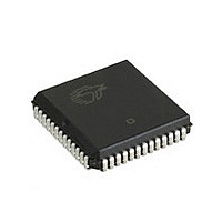
CY7C131-55JCT Cypress Semiconductor Corp, CY7C131-55JCT Datasheet - Page 10

CY7C131-55JCT
Manufacturer Part Number
CY7C131-55JCT
Description
Manufacturer
Cypress Semiconductor Corp
Datasheet
1.CY7C131-55JCT.pdf
(19 pages)
Specifications of CY7C131-55JCT
Density
8Kb
Access Time (max)
55ns
Sync/async
Asynchronous
Architecture
Not Required
Clock Freq (max)
Not RequiredMHz
Operating Supply Voltage (typ)
5V
Address Bus
20b
Package Type
PLCC
Operating Temp Range
0C to 70C
Number Of Ports
2
Supply Current
110mA
Operating Supply Voltage (min)
4.5V
Operating Supply Voltage (max)
5.5V
Operating Temperature Classification
Commercial
Mounting
Surface Mount
Pin Count
52
Word Size
8b
Number Of Words
1K
Lead Free Status / RoHS Status
Not Compliant
Switching Waveforms
Document #: 38-06002 Rev. *F
Notes
ADDRESS
23. If OE is LOW during a R/W controlled write cycle, the write pulse width must be the larger of t
24. If the CE LOW transition occurs simultaneously with or after the R/W LOW transition, the outputs remain in the high impedance state.
ADDRESS
DATA
DATA
D
DATA
and for data to be placed on the bus for the required t
OUT
R/W
OE
CE
R/W
IN
OUT
CE
IN
Figure 9. Write Cycle No. 2 (R/W Three-States Data I/Os—Either Port)
Figure 8. Write Cycle No. 1 (OE Three-States Data I/Os—Either Port
t
HZOE
t
SA
(continued)
t
SA
SD
.
t
SCE
t
SCE
t
AW
t
AW
t
Either Port
HZWE
t
WC
t
WC
HIGH IMPEDANCE
t
PWE
DATA VALID
t
PWE
t
SD
PWE
HIGH IMPEDANCE
or t
t
DATA VALID
SD
HZWE
+ t
SD
to allow the data I/O pins to enter high impedance
t
HD
t
HD
t
LZWE
t
HA
t
HA
CY7C130, CY7C130A
CY7C131, CY7C131A
[16, 23]
[17, 24]
Page 10 of 19
[+] Feedback
[+] Feedback


