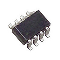
LTC2927ITS8#PBF Linear Technology, LTC2927ITS8#PBF Datasheet - Page 5

LTC2927ITS8#PBF
Manufacturer Part Number
LTC2927ITS8#PBF
Description
Manufacturer
Linear Technology
Datasheet
1.LTC2927ITS8PBF.pdf
(16 pages)
Specifications of LTC2927ITS8#PBF
Operating Temperature (max)
85C
Operating Temperature (min)
-40C
Pin Count
8
Mounting
Surface Mount
Package Type
TSOT-23
Case Length
2.9mm
Screening Level
Industrial
Lead Free Status / RoHS Status
Compliant
Available stocks
Company
Part Number
Manufacturer
Quantity
Price
PI FU CTIO S
GND (Pin 4/Pin 5): Device Ground.
TRACK (Pin 5/Pin 4): Tracking Control Input. A resistive
voltage divider between RAMPBUF and TRACK determines
the tracking profi le of the slave supply. TRACK servos to
0.8V, and the current supplied at TRACK is mirrored at FB.
The TRACK pin is capable of supplying at least 1mA when
V
is capable of supplying up to 70mA. Do not connect to
GND for extended periods. Limit the capacitance at the
TRACK pin to less than 25pF .
RAMPBUF (Pin 6/Pin 3): Ramp Buffer Output. Provides
a low impedance buffered version of the signal on the
RAMP pin. This buffered output drives the resistive volt-
age divider that connects to the TRACK pin. Limit the
capacitance at the RAMPBUF pin to less than 100pF . Float
RAMPBUF if unused.
FU CTIO AL BLOCK DIAGRA
CC
U
U
= 2.9V. Under short circuit conditions, the TRACK pin
U
U
U
TSOT/DFN Packages
5
5
5
1.23V
RAMPBUF
ON
TRACK
2.5V
V
CC
+
–
+
–
UVLO
W
+
–
GND
V
V
5
CC
CC
5
RAMP (Pin 7/Pin 2): Ramp Buffer Input. The RAMP pin is
the input to the voltage buffer whose output drives a resis-
tive voltage divider connected to the TRACK pin. Connect
this input to a capacitor to set the ramp voltage generated
from internal 10μA pull-up or pull-down currents. RAMP
can also be connected to an external ramping signal for
tracking. Ground RAMP if unused.
ON (Pin 8/Pin 1): On Control Input. The voltage level of
the ON pin relative to its 1.23V threshold (with 75mV
hysteresis) controls the tracking direction of the LTC2927.
An active high causes a 10μA pull-up current to fl ow at
the RAMP pin, which charges an external capacitor. An
active low at the ON pin causes a 10μA pull-down cur-
rent at the RAMP pin to discharge the external capacitor
relative to GND.
Exposed Pad (NA/Pin 9): Exposed pad may be left open
or connected to device ground.
1x
0.8V
–
+
10μA
10μA
0.2V
V
CC
RAMP
SDO
FB
2927 BD
5
5
5
LTC2927
2927fb
5


