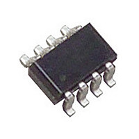
LTC2927ITS8#PBF Linear Technology, LTC2927ITS8#PBF Datasheet - Page 8

LTC2927ITS8#PBF
Manufacturer Part Number
LTC2927ITS8#PBF
Description
Manufacturer
Linear Technology
Datasheet
1.LTC2927ITS8PBF.pdf
(16 pages)
Specifications of LTC2927ITS8#PBF
Operating Temperature (max)
85C
Operating Temperature (min)
-40C
Pin Count
8
Mounting
Surface Mount
Package Type
TSOT-23
Case Length
2.9mm
Screening Level
Industrial
Lead Free Status / RoHS Status
Compliant
Available stocks
Company
Part Number
Manufacturer
Quantity
Price
APPLICATIO S I FOR ATIO
LTC2927
SDO pulls low again when the ON pin is pulled below 1.23V
and the RAMP pin is below about 200mV.
3-Step Design Procedure
The following 3-step procedure allows one to complete
a design for any of the tracking or sequencing profi les
shown in Figures 1 to 4. A basic single supply application
circuit is shown in Figure 8.
1. Set the ramp rate of the master signal.
2. Solve for the pair of resistors that provide the desired
8
Solve for the value of C
pin, based on the desired ramp rate (V/s) of the master
supply, S
ramp rate of the slave supply, assuming no delay.
C
RAMP
EARLY
EARLY
3.3V
V
R
R
V
IN
16.5k
R
R
ONB
ONA
R
138k
100k
R
IN
ONB
ONA
R
R
13k
TB
TA
TB
TA
=
M
Figure 7. SDO Shutdown Application
I
Figure 8. Single Supply Application
RAMP
.
S
ON
RAMPBUF
TRACK
ON
RAMPBUF
TRACK
M
0.1μF
0.1μF
LTC2927
LTC2927
U
GND
V
GND
where I
V
CC
CC
RAMP
RAMP
2927 F08
SDO
RAMP
2927 F07
FB
FB
U
RAMP
, the capacitor on the RAMP
R
R
35.7k
FA
FA
C
FB
C
10pF
RAMP
RUN/SS
FB = 1.235V
RAMP
≈
10
W
DC/DC
DC/DC
R
V
16.5k
IN
MASTER
R
V
μ
IN
FB
IN
MASTER
FB
IN
A
OUT
OUT
U
SLAVE
1.8V
1 ( )
3. Choose R
As noted in step 2, small delays and large ratios of slave ramp
rate to master ramp rate (usually only seen in sequencing)
may result in solutions with negative values for R
cases, either the delay must be increased or the ratio of
slave ramp rate to master ramp rate must be reduced.
Choose a ramp rate for the slave supply, S
supply ramps up coincident with the master signal or
with a fi xed voltage offset, then the ramp rate equals
the master supply’s ramp rate. Be sure to use a fast
enough ramp rate for the slave supply so that it will fi nish
ramping before the master signal has reached its fi nal
supply value. If not, the slave supply will be held below
the intended regulation value by the master signal. Use
the following formulas to determine the resistor values
for the desired ramp rate, where R
feedback resistors in the slave supply and V
feedback reference voltage of the slave supply:
where V
Note that large ratios of slave ramp rate to master ramp
rate, S
suffi ciently large delay is used in step 3, R
positive, otherwise S
If no delay is required, such as in coincident and ratio-
metric tracking, then simply set R
is desired, as in offset tracking and supply sequencing,
calculate R
is the desired delay in seconds.
the parallel combination of R
R
R
R
R
TB
TA
TA
TA
′ =
″ =
=
=
S
R
R
/S
TRACK
R
V
FB
V
TA
FB
FB
TA
M
TRACK
TA
′
•
, may result in negative values for R
t
to obtain the desired delay.
D
||
+
” to determine the value of R
S
S
R
≈ 0.8V.
•
M
S
R
V
V
TA
S
TRACK
FB
•
FA
M
R
″
−
TB
S
V
/S
TRACK
R
M
TB
must be reduced.
TA
’ and R
TA
FB
= R
and R
TA
”.
TA
S
. If the slave
TA
’. If a delay
TA
FA
TA
where t
FB
. In such
are the
will be
is the
TA
2927fb
’. If
( ) 3
( ) 4
( ) 2
( ) 5
D


