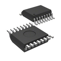
MIC74BQS Micrel Inc, MIC74BQS Datasheet - Page 8

MIC74BQS
Manufacturer Part Number
MIC74BQS
Description
IC I/O EXPANDER I2C 8B 16QSOP
Manufacturer
Micrel Inc
Series
-r
Datasheet
1.MIC74YQS.pdf
(18 pages)
Specifications of MIC74BQS
Interface
I²C, SMBus
Number Of I /o
8
Interrupt Output
Yes
Frequency - Clock
-
Voltage - Supply
2.7 V ~ 3.6 V
Operating Temperature
-40°C ~ 85°C
Mounting Type
Surface Mount
Package / Case
16-SSOP (0.154", 3.90mm Width)
Includes
-
Lead Free Status / Rohs Status
Contains lead / RoHS non-compliant
Pn, /SHDN, and /FS0–/FS2
P0 through P7 are general-purpose input/output bits.
Each bit is independently programmable as an input or
an output. If programmed as an output, each bit is
further programmable as either a complementary push-
pull or open-drain output.
If properly enabled, any Pn programmed as an input will
generate an interrupt to the host using the /ALERT
output when the input changes state. In this way, the
MIC74 can notify the host of an input change without
requiring periodic polling by the host or a message
transaction on the bus.
Regardless of whether interrupts are enabled or
disabled, each input-change event also sets the
corresponding bit in the status register. I/O configuration
is performed using the output configuration (OUT_CFG),
I/O direction (DIR), and interrupt mask (INT_MASK)
registers.
If the FAN bit in the device configuration register is set,
the states of P[7:4] are controlled by the FAN_SPEED
register. The bits in the OUT_CFG, DIR, and INT_MASK
registers corresponding to P[7:4] are ignored. When in
Fan Mode, P[7:4] are referred to as /FS2, /FS1, /FS0,
and /SHDN. While in this mode, no interrupts of any kind
will be generated by these pins.
/ALERT
The alert signal is an open-drain, active-low output. The
operation of the /ALERT output is controlled by the IMn
bits in the INT_MASK register and the global interrupt
enable bit (IE) in the DEV_CFG register.
If the IE bit is set to zero, or if the corresponding interrupt
enable bit, IMn, is set to zero, no input-change interrupts
will be generated. (Regardless of the IE bit setting, the
change will be reflected in the status register.)
If the IE bit is set to one, IMn is set to one, and Pn is an
input, then /ALERT is driven active whenever Pn
changes state, (goes from a high-to-low or low-to-high
state). Once triggered, /ALERT is unconditionally reset
to its inactive state once the MIC74 successfully
responds to the alert response addressor STATUS is
read.
Serial Port Operation
The MIC74 uses standard SMBus Read_Byte and
Write_Byte operations to communicate with its host.
The Read_Byte operation is a composite read-write
operation consisting of first sending the MIC74’s slave
address followed by a command byte (a write) and then
resending the slave address and clocking out the data
byte (a read). The command byte is the address of the
target register. See Table 2. An example of a Read_Byte
operation is shown in Figure 8.
Micrel, Inc.
October 2006
8
Similarly, the write-byte operation consists of sending
the device’s slave address followed by a command byte
and the byte to be written to the target register. Again, in
the case of the MIC74, the command byte is the address
of the target register. See Table 2.
In addition, to the read byte and write byte protocols, the
MIC74 adheres to the SMBus protocol for response to
the ARA (alert response address). An MIC74 expects to
be interrogated using the ARA when it has asserted its
/ALERT output. /ALERT interrupts can be enabled or
disabled using the IE bit in the DEV_CFG register.
Power-On
When power is initially applied, the MIC74’s internal
registers will assume their power-up default state and
the state of the address inputs, A2, A1 and A0, will be
read to establish the device’s slave address. See the
individual register descriptions for each registers default
state. Also see Table 2.
I/O Ports
Each I/O bit, P0 through P7, may be individually
programmed
corresponding bit in the I/O direction register, DIR.
If
programmable as either a complementary push-pull or
open-drain output using the output configuration register,
OUT_CFG.
If enabled by the corresponding bit, IMn, in the interrupt
mask register INT_MASK, each Pn programmed as an
input will generate an interrupt to the host on /ALERT if
the input changes state. In this way, the MIC74 can
notify the host of an input change without requiring
periodic polling by the host or a transaction on the bus.
Each input-change event also sets the corresponding bit
in the status register, STATUS.
See “Functional Diagram” for the logic arrangement of
atypical MIC74 I/O port.
Fan Speed Control
If the FAN bit in the device configuration register is set,
the state of P[7:4] is controlled by the FAN_SPEED
register. The bits in the OUT_CFG, DIR, and INT_MASK
registers corresponding to P[7:4] are ignored. When in
Fan Control Mode, P[7:4] are referred to as /FS2, /FS1,
/FS0, and /SHDN. While in this mode, no interrupts of
any kind will be generated by these pins. See
“Applications Information” for typical fan speed control
applications.
programmed
as
as
an
an
input
output,
or
output
each
M9999-101006
using
is
MIC74
further
the


