W40S01-04H Cypress Semiconductor Corp, W40S01-04H Datasheet
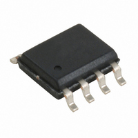
IC CLK BUFF 18OUT SDRAM 48SSOP

W40S01-04H

Manufacturer Part Number
W40S01-04H
Description
IC CLK BUFF 18OUT SDRAM 48SSOP
Manufacturer
Cypress Semiconductor Corp
Type
Clock Bufferr
Datasheet

Specifications of W40S01-04H

Input
Crystal or Other
Output
CMOS
Frequency - Max
133MHz
Voltage - Supply
3.135 V ~ 3.465 V
Operating Temperature
0°C ~ 70°C
Mounting Type
Surface Mount
Package / Case
48-SSOP
Frequency-max
133MHz
Lead Free Status / RoHS Status
Contains lead / RoHS non-compliant
Other names
428-1400

Available stocks

Company
Part Number
Manufacturer
Quantity
Price
Part Number:
W40S01-04H
Manufacturer:
CYPRESS
Quantity:
90
Part Number:
W40S01-04H
Manufacturer:
WORKS
Quantity:
20 000
Features
Overview
The Cypress W40S01-04 is a low-voltage, eighteen-output
signal buffer. Output buffer impedance is approximately 15
which is ideal for driving SDRAM DIMMs.
Intel is a registered trademark of Intel Corporation.
Cypress Semiconductor Corporation
• Eighteen skew controlled CMOS outputs (SDRAM0:17)
• Supports four SDRAM DIMMs
• Ideal for high-performance systems designed around
• SMBus serial configuration interface
• Output skew between any two outputs is less than
• 1 to 5 ns propagation delay
• DC to 133-MHz operation
• Single 3.3V supply voltage
• Low power CMOS design packaged in a 48-pin SSOP
Block Diagram
Intel®’s 440BX chip set
250 ps
(Small Shrink Outline Package)
SCLOCK
BUF_IN
SDATA
Serial Port
Device Control
3901 North First Street
SDRAM0
SDRAM1
SDRAM2
SDRAM3
SDRAM4
SDRAM5
SDRAM6
SDRAM7
SDRAM8
SDRAM9
SDRAM10
SDRAM11
SDRAM12
SDRAM13
SDRAM14
SDRAM15
SDRAM16
SDRAM17
OE
Key Specifications
Supply Voltages:..................................... V
Operating Temperature:.................................... 0°C to +70°C
Input Threshold: .................................................. 1.5V typical
Maximum Input Voltage: ...................................V
Input Frequency:............................................... 0 to 133 MHz
BUF_IN to SDRAM0:17 Propagation Delay: ......1.0 to 5.0 ns
Output Edge Rate:.................................................. >1.5 V/ns
Output Skew: ............................................................ ±250 ps
Output Duty Cycle: .................................. 45/55% worst case
Output Impedance:...............................................15 typical
Output Type: ................................................ CMOS rail-to-rail
Part to Part Skew:........................................................700 ps
Pin Configuration
Note:
1.
SDRAM16
SDRAM0
SDRAM1
SDRAM2
SDRAM3
SDRAM4
SDRAM5
SDRAM6
SDRAM7
Internal pull-up resistor of 250K on SDATA, SCLOCK, and OE
inputs (not CMOS level).
SDATA
BUF_IN
VDDQ3
VDDQ3
VDDQ3
VDDQ3
VDDQ3
VDDQ3
San Jose
SDRAM Buffer - 4 DIMM
GND
GND
GND
GND
GND
NC
NC
[1]
1
2
3
4
5
6
7
8
9
10
11
12
13
14
15
16
17
18
19
20
21
22
23
24
CA 95134
SSOP
48
47
46
45
44
43
42
41
40
39
38
37
36
35
34
33
32
31
30
29
28
27
26
25
W40S01-04
DDQ3
NC
NC
VDDQ3
SDRAM15
SDRAM14
GND
VDDQ3
SDRAM13
SDRAM12
GND
OE
VDDQ3
SDRAM11
SDRAM10
GND
VDDQ3
SDRAM9
SDRAM8
GND
VDDQ3
SDRAM17
GND
GND
SCLOCK
408-943-2600
= 3.3V ± 5%
DDQ3
April 5, 2001
[1]
+ 0.5V
[1]

Related parts for W40S01-04H

W40S01-04H Summary of contents

Page 1

... DC to 133-MHz operation • Single 3.3V supply voltage • Low power CMOS design packaged in a 48-pin SSOP (Small Shrink Outline Package) Overview The Cypress W40S01- low-voltage, eighteen-output signal buffer. Output buffer impedance is approximately 15 which is ideal for driving SDRAM DIMMs. Block Diagram SDATA ...

Page 2

... SMBus section of this data sheet. Internal 250-k pull-up resistor. Power Connection: Power supply for core logic and output buffers. Connected to 3.3V supply. Ground Connection: Connect all ground pins to the common system ground plane. Output Enable: Internal 250-k pull-up resistor. Three-states outputs when LOW. No Connect: Do not connect. 2 W40S01- ...

Page 3

... Data is written to the W40S01-04 in ten bytes of eight bits each. Bytes are written in the order shown in Table 1. Byte Description Commands the W40S01-04 to accept the bits in Data Bytes 0-6 for inter- nal register configuration. Since other devices may exist on the same common serial data bus necessary to have a specific slave address for each potential receiver ...

Page 4

... Clock Output Disable Clock Output Disable Clock Output Disable Clock Output Disable Clock Output Disable Clock Output Disable Clock Output Disable (Reserved) (Reserved) (Reserved) (Reserved) (Reserved) (Reserved) 4 W40S01-04 Bit Control 0 1 Low Active Low Active Low Active Low Active Low Active ...

Page 5

... Electrical Requirements Figure 1 illustrates electrical characteristics for the serial inter- face bus used with the W40S01-04. Devices send data over the bus with an open drain logic output that can (a) pull the bus line LOW, or (b) let the bus default to logic 1. The pull-up resis- ...

Page 6

... A write sequence is initiated by a “start bit” as shown in Figure 3. A “stop bit” signifies that a transmission has ended. As stated previously, the W40S01-04 sends an “acknowledge” pulse after receiving eight data bits in each byte as shown in Figure 4. SDATA ...

Page 7

... Figure 4. Serial Data Bus Write Sequence Figure 5. Serial Data Bus Timing Diagram 7 W40S01-04 ...

Page 8

... V = 3.3V ± DDQ3 Test Condition/ Comments BUF_IN = 100 MHz BUF_IN = 100 MHz [ – 1. 1. W40S01-04 Rating Unit –0.5 to +7.0 V –65 to +150 ° +70 °C –55 to +125 °C Min. Typ. Max. Unit 320 5 GND–0.3 0.8 2.0 V +0.5 DDQ3 – ...

Page 9

... Capacitance Test Load = 30 pF) A DDQ3 Test Condition Measured from 0.4V to 2.4V Measured from 2.4V to 0.4V Measured at 1.5V Package Name Package Type H 48-pin SSOP (300 mils) 9 W40S01-04 Min. Typ. Max. Unit 0 133 MHz 1.5 4.0 V/ns 1.5 4.0 V/ns ...

Page 10

... Layout Example SDATA VIA to GND plane layer +3.3V Supply =VIA to supply plane layer 10 W40S01- SCLOCK ...

Page 11

... The inclusion of Cypress Semiconductor products in life-support systems application implies that the manufacturer assumes all risk of such use and in doing so indemnifies Cypress Semiconductor against all charges. W40S01-04 ...

Related keywords