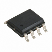
W40S01-04H Cypress Semiconductor Corp, W40S01-04H Datasheet - Page 4

W40S01-04H
Manufacturer Part Number
W40S01-04H
Description
IC CLK BUFF 18OUT SDRAM 48SSOP
Manufacturer
Cypress Semiconductor Corp
Type
Clock Bufferr
Datasheet
1.W40S01-04H.pdf
(11 pages)
Specifications of W40S01-04H
Input
Crystal or Other
Output
CMOS
Frequency - Max
133MHz
Voltage - Supply
3.135 V ~ 3.465 V
Operating Temperature
0°C ~ 70°C
Mounting Type
Surface Mount
Package / Case
48-SSOP
Frequency-max
133MHz
Lead Free Status / RoHS Status
Contains lead / RoHS non-compliant
Other names
428-1400
Available stocks
Company
Part Number
Manufacturer
Quantity
Price
Company:
Part Number:
W40S01-04H
Manufacturer:
CYPRESS
Quantity:
90
Part Number:
W40S01-04H
Manufacturer:
WORKS
Quantity:
20 000
Writing Data Bytes
Each bit in the data bytes control a particular device function.
Bits are written MSB (most significant bit) first, which is bit 7.
Table 2. Data Bytes 0–2 Serial Configuration Map
Note:
2.
Data Byte 0 SDRAM Active/Inactive Register (1 = Enable, 0 = Disable)
Data Byte 1 SDRAM Active/Inactive Register (1 = Enable, 0 = Disable)
Data Byte 2 SDRAM Active/Inactive Register (1 = Enable, 0 = Disable)
At power-up all SDRAM outputs are enabled and active. Program Reserved bits to 0.
Bit(s)
7
6
5
4
3
2
1
0
7
6
5
4
3
2
1
0
7
6
5
4
3
2
1
0
Pin No.
N/A
N/A
N/A
N/A
N/A
N/A
18
17
14
13
45
44
41
40
36
35
32
31
28
21
9
8
5
4
Affected Pin
SDRAM15
SDRAM14
SDRAM13
SDRAM12
SDRAM11
SDRAM10
SDRAM17
SDRAM16
Pin Name
Reserved
Reserved
Reserved
Reserved
Reserved
Reserved
SDRAM7
SDRAM6
SDRAM5
SDRAM4
SDRAM3
SDRAM2
SDRAM1
SDRAM0
SDRAM9
SDRAM8
Clock Output Disable
Clock Output Disable
Clock Output Disable
Clock Output Disable
Clock Output Disable
Clock Output Disable
Clock Output Disable
Clock Output Disable
Clock Output Disable
Clock Output Disable
Clock Output Disable
Clock Output Disable
Clock Output Disable
Clock Output Disable
Clock Output Disable
Clock Output Disable
Clock Output Disable
Clock Output Disable
(Reserved)
(Reserved)
(Reserved)
(Reserved)
(Reserved)
(Reserved)
Control Function
[2]
4
Table 2 gives the bit formats for registers located in Data
Bytes 0–6.
Low
Low
Low
Low
Low
Low
Low
Low
Low
Low
Low
Low
Low
Low
Low
Low
Low
Low
--
--
--
--
--
--
0
Bit Control
W40S01-04
Active
Active
Active
Active
Active
Active
Active
Active
Active
Active
Active
Active
Active
Active
Active
Active
Active
Active
--
--
--
--
--
--
1


