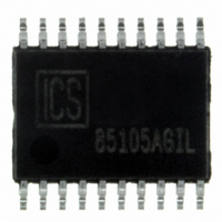
ICS85105AGILF IDT, Integrated Device Technology Inc, ICS85105AGILF Datasheet - Page 9

ICS85105AGILF
Manufacturer Part Number
ICS85105AGILF
Description
IC FANOUT BUFFER HCSL 20-TSSOP
Manufacturer
IDT, Integrated Device Technology Inc
Series
HiPerClockS™r
Type
Fanout Buffer (Distribution), Multiplexerr
Specifications of ICS85105AGILF
Number Of Circuits
1
Ratio - Input:output
2:5
Differential - Input:output
Yes/Yes
Input
HCSL, LVCMOS, LVDS, LVHSTL, LVPECL, LVTTL, SSTL
Output
HCSL
Frequency - Max
500MHz
Voltage - Supply
2.97 V ~ 3.63 V
Operating Temperature
-40°C ~ 85°C
Mounting Type
Surface Mount
Package / Case
20-TSSOP
Frequency-max
500MHz
Number Of Clock Inputs
2
Output Frequency
500MHz
Output Logic Level
HCSL
Operating Supply Voltage (min)
2.97V
Operating Supply Voltage (typ)
3.3V
Operating Supply Voltage (max)
3.63V
Package Type
TSSOP
Operating Temp Range
-40C to 85C
Operating Temperature Classification
Industrial
Mounting
Surface Mount
Pin Count
20
Lead Free Status / RoHS Status
Lead free / RoHS Compliant
Other names
800-1152
800-1152-5
800-1152
85105AGILF
800-1152-5
800-1152
85105AGILF
Figure 2 shows how a differential input can be wired to accept
single ended levels. The reference voltage V
generated by the bias resistors R1 and R2. The bypass capacitor
(C1) is used to help filter noise on the DC bias. This bias circuit
should be located as close to the input pin as possible. The ratio
of R1 and R2 might need to be adjusted to position the V
center of the input voltage swing. For example, if the input clock
swing is 2.5V and V
to set V
ended swing and V
requires that the sum of the output impedance of the driver (Ro)
and the series resistance (Rs) equals the transmission line
impedance. In addition, matched termination at the input will
attenuate the signal in half. This can be done in one of two ways.
First, R3 and R4 in parallel should equal the transmission line
ICS85105I Data Sheet
R
I
CLK I
For applications not requiring the use of a clock input, it can be
left floating. Though not required, but for additional protection, a
1k
CLK/nCLK I
For applications not requiring the use of the differential input, both
CLK and nCLK can be left floating. Though not required, but for
additional protection, a 1k
ground.
LVCMOS C
All control pins have internal pull-ups or pull-downs; additional
resistance is not required but can be added for additional
protection. A 1k
W
ICS85105AGI REVISION A MAY 27, 2011
NPUTS
ECOMMENDATIONS FOR
IRING THE
resistor can be tied from the CLK input to ground.
NPUT
REF
:
at 1.25V. The values below are for when both the single-
ONTROL
NPUTS
D
IFFERENTIAL
resistor can be used.
DD
P
DD
INS
= 3.3V, R1 and R2 value should be adjusted
are at the same voltage. This configuration
U
NUSED
resistor can be tied from CLK to
I
NPUT TO
F
I
A
NPUT AND
IGURE
A
PPLICATIONS
CCEPT
2. S
REF
O
S
INGLE
INGLE
UTPUT
= V
REF
E
DD
NDED
in the
E
/2 is
P
NDED
INS
I
S
NFORMATION
IGNAL
LOW SKEW, 1-TO-5, DIFFERENTIAL/LVCMOS-TO-0.7V HCSL FANOUT BUFFER
9
L
O
D
All unused differential outputs can be left floating. We recommend
that there is no trace attached. Both sides of the differential output
pair should either be left floating or terminated.
impedance. For most 50 applications, R3 and R4 can be 100 .
The values of the resistors can be increased to reduce the loading
for slower and weaker LVCMOS driver. When using single ended
signaling, the noise rejection benefits of differential signaling are
reduced. Even though the differential input can handle full rail
LVCMOS signaling, it is recommended that the amplitude be
reduced. The datasheet specifies a lower differential amplitude,
however this only applies to differential signals. For single-ended
applications, the swing can be larger, however V
than -0.3V and V
of the recommended components might not be used, the pads
should be placed in the layout. They can be utilized for debugging
purposes. The datasheet specifications are characterized and
guaranteed by using a differential signal.
EVELS
IFFERENTIAL
UTPUTS
D
RIVING
:
D
O
IFFERENTIAL
UTPUT
IH
cannot be more than V
s
I
NPUT
2011 Integrated Device Technology, Inc.
DD
+ 0.3V. Though some
IL
cannot be less


