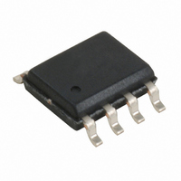
CY25560SXC Cypress Semiconductor Corp, CY25560SXC Datasheet - Page 3

CY25560SXC
Manufacturer Part Number
CY25560SXC
Description
IC CLOCK GEN 3.3V SS 8-SOIC
Manufacturer
Cypress Semiconductor Corp
Type
Clock/Frequency Synthesizer, Frequency Modulator, Spread Spectrum Clock Generatorr
Datasheet
1.CY25560SXC.pdf
(9 pages)
Specifications of CY25560SXC
Number Of Circuits
1
Package / Case
8-SOIC (3.9mm Width)
Pll
Yes
Input
Clock, Crystal
Output
Clock
Ratio - Input:output
1:1
Differential - Input:output
No/No
Frequency - Max
100MHz
Divider/multiplier
Yes/No
Voltage - Supply
2.97 V ~ 3.63 V
Operating Temperature
0°C ~ 70°C
Mounting Type
Surface Mount
Frequency-max
100MHz
Maximum Input Frequency
100 MHz
Minimum Input Frequency
25 MHz
Supply Voltage (max)
3.63 V
Supply Voltage (min)
2.97 V
Maximum Operating Temperature
+ 70 C
Minimum Operating Temperature
0 C
Mounting Style
SMD/SMT
Operating Supply Voltage
3.3 V
Lead Free Status / RoHS Status
Lead free / RoHS Compliant
Lead Free Status / RoHS Status
Lead free / RoHS Compliant, Lead free / RoHS Compliant
Other names
428-2222-5
CY25560SXC
CY25560SXC
Available stocks
Company
Part Number
Manufacturer
Quantity
Price
Company:
Part Number:
CY25560SXC
Manufacturer:
CY
Quantity:
1 262
Part Number:
CY25560SXC
Manufacturer:
CYP
Quantity:
20 000
Company:
Part Number:
CY25560SXCT
Manufacturer:
CYPRESS
Quantity:
1 710
Part Number:
CY25560SXCT
Manufacturer:
CYPRESS/赛普拉斯
Quantity:
20 000
Tri-Level Logic
With binary logic, four states can be programmed with two
control lines, whereas three-level logic can program nine logic
states using two control lines. Three-level logic in the CY25560
is implemented by defining a third logic state in addition to the
standard logic ‘1’ and ‘0’. Pins 6 and 7 of the CY25560 recognize
a logic state by the voltage applied to their respective pin. These
states are defined as ‘0’ (Low), ‘M’ (Middle), and ‘1’ (One). Each
of these states have a defined voltage range that is interpreted
by the CY25560 as a ‘0’, ‘M’, or ‘1’ logic state. Refer to
for voltage ranges for each logic state. The CY25560 has two
equal value resistor dividers connected internally to Pins 6 and
7 that produce the default ‘M’ (Middle) state if these pins are left
unconnected (NC). Pins 6 and/or 7 can be tied directly to ground
or V
SSCG Theory of Operation
The CY25560 is a PLL-type clock generator using a proprietary
Cypress design. By precisely controlling the bandwidth of the
output clock, the CY25560 becomes a low-EMI clock generator.
Document #: 38-07425 Rev. *F
Table 2. Frequency and Spread% Selection
DD
SSCC = "1"
S1 = "0" (GND)
S0 = "M" (N/C)
to program a logic ‘0’ or ‘1’ state, respectively.
CY25560
7
6
5
Frequency
Frequency
S0
VDD
S1
80 – 100
25 – 35
35 – 40
40 – 45
45 – 50
50 – 60
60 – 70
70 – 80
(MHz)
(MHz)
Input
Input
S1=M
S0=M
S0=M
S1=1
(%)
(%)
4.3
3.9
3.7
3.4
2.9
2.8
2.6
2.4
Figure 2. Three-Level Logic Examples
S1=M
S0=0
S1=0
S0=1
(%)
(%)
3.8
3.5
3.3
3.1
2.1
2.0
1.8
1.7
50 – 100 MHz (High Range)
25 – 50 MHz (Low Range)
S1 = "0" (GND)
SSCC = "1"
CY25560
S0 = "1"
Table 3
S1=1
S0=0
S1=1
S0=1
(%)
(%)
3.4
3.1
2.8
2.6
1.5
1.4
1.3
1.2
7
6
5
The theory and detailed operation of the CY25560 is discussed
in the following sections.
EMI
All digital clocks generate unwanted energy in their harmonics.
Conventional digital clocks are square waves with a duty cycle
that is very close to 50%. Because of this 50/50 duty cycle, digital
clocks generate most of their harmonic energy in the odd
harmonics, i.e., third, fifth, seventh, etc. It is possible to reduce
the amount of energy contained in the fundamental and odd
harmonics by increasing the bandwidth of the fundamental clock
frequency. Conventional digital clocks have a very high Q factor,
which means that all of the energy at that frequency is
concentrated in a very narrow bandwidth, consequently, higher
energy peaks. Regulatory agencies test electronic equipment by
the amount of peak energy radiated from the equipment. By
reducing the peak energy at the fundamental and harmonic
frequencies, the equipment under test is able to satisfy agency
requirements for EMI. Conventional methods of reducing EMI
have been to use shielding, filtering, multilayer PCBs, etc. The
CY25560 uses the approach of reducing the peak energy in the
clock by increasing the clock bandwidth, and lowering the Q
factor.
S0
VDD
S1
S1=M
S1=0
S0=0
S0=1
(%)
(%)
2.9
2.5
2.4
2.2
1.2
1.1
1.1
1.0
VDD
S0=M
S1=0
(%)
2.8
2.4
2.3
2.1
Select the
Frequency and
Center Spread %
desired and then
set S1, S0 as
indicated.
Select the
Frequency and
Center Spread %
desired and then
set S1, S0 as
indicated.
CY25560
S0 = "1"
S1 = "1"
SSCC = "1"
7
6
5
CY25560
S1
S0
Page 3 of 9
VDD
[+] Feedback


