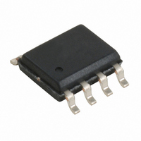
CY25560SXC Cypress Semiconductor Corp, CY25560SXC Datasheet - Page 4

CY25560SXC
Manufacturer Part Number
CY25560SXC
Description
IC CLOCK GEN 3.3V SS 8-SOIC
Manufacturer
Cypress Semiconductor Corp
Type
Clock/Frequency Synthesizer, Frequency Modulator, Spread Spectrum Clock Generatorr
Datasheet
1.CY25560SXC.pdf
(9 pages)
Specifications of CY25560SXC
Number Of Circuits
1
Package / Case
8-SOIC (3.9mm Width)
Pll
Yes
Input
Clock, Crystal
Output
Clock
Ratio - Input:output
1:1
Differential - Input:output
No/No
Frequency - Max
100MHz
Divider/multiplier
Yes/No
Voltage - Supply
2.97 V ~ 3.63 V
Operating Temperature
0°C ~ 70°C
Mounting Type
Surface Mount
Frequency-max
100MHz
Maximum Input Frequency
100 MHz
Minimum Input Frequency
25 MHz
Supply Voltage (max)
3.63 V
Supply Voltage (min)
2.97 V
Maximum Operating Temperature
+ 70 C
Minimum Operating Temperature
0 C
Mounting Style
SMD/SMT
Operating Supply Voltage
3.3 V
Lead Free Status / RoHS Status
Lead free / RoHS Compliant
Lead Free Status / RoHS Status
Lead free / RoHS Compliant, Lead free / RoHS Compliant
Other names
428-2222-5
CY25560SXC
CY25560SXC
Available stocks
Company
Part Number
Manufacturer
Quantity
Price
Company:
Part Number:
CY25560SXC
Manufacturer:
CY
Quantity:
1 262
Part Number:
CY25560SXC
Manufacturer:
CYP
Quantity:
20 000
Company:
Part Number:
CY25560SXCT
Manufacturer:
CYPRESS
Quantity:
1 710
Part Number:
CY25560SXCT
Manufacturer:
CYPRESS/赛普拉斯
Quantity:
20 000
SSCG
SSCG uses a patented technology of modulating the clock over
a very narrow bandwidth and controlled rate of change, both
peak and cycle-to-cycle. The CY25560 takes a narrow band
digital reference clock in the range of 25 to 100 MHz and
produces a clock that sweeps between a controlled start and
stop frequency and precise rate of change. To understand what
happens to a clock when SSCG is applied, consider a 65 MHz
clock with a 50% duty cycle. From a 65 MHz clock we know the
following:
If this clock is applied to the Xin/CLK pin of CY25560, the output
clock at Pin 4 (SSCLK) sweeps back and forth between two
frequencies. These two frequencies, F1 and F2, are used to
calculate to total amount of spread or bandwidth applied to the
reference clock at Pin 1. As the clock is making the transition
from F1 to F2, the amount of time and sweep waveform play a
very important role in the amount of EMI reduction realized from
an SSCG clock.
Document #: 38-07425 Rev. *F
Clock frequency = fc = 65 MHz
Clock period = Tc =1/65 MHz = 15.4 ns
Device
CY25560
Example:
Then:
Device =
Fin
Range =
Modulation Rate = Fmod = 65 MHz/1166 = 55.7 kHz.
=
Modulation Profile
Divider Count (Cdiv)
1166 (All Ranges)
CY25560
65 MHz
S1 = 1, S0 = 0
50 %
Tc = 15.4 ns
Figure 3. SSCG Clock, CY25560, Fin = 65 MHz
50 %
The modulation domain analyzer is used to visualize the sweep
waveform and sweep period.
profile of a 65 MHz SSCG clock. Notice that the actual sweep
waveform is not a simple sine or sawtooth waveform.
also shows a scan of the same SSCG clock using a spectrum
analyzer. In this scan you can see a 6.48 dB reduction in the
peak RF energy when using the SSCG clock.
Modulation Rate
Spectrum Spread Clock Generators utilize frequency modulation
(FM) to distribute energy over a specific band of frequencies. The
maximum frequency of the clock (Fmax) and minimum
frequency of the clock (Fmin) determine this band of frequencies.
The time required to transition from Fmin to Fmax and back to
Fmin is the period of the Modulation Rate, Tmod. Modulation
Rates of SSCG clocks are generally referred to in terms of
frequency or Fmod = 1/Tmod.
The input clock frequency, Fin, and the internal divider count,
Cdiv, determine the Modulation Rate. In some SSCG clock
generators, the selected range determines the internal divider
count. In other SSCG clocks, the internal divider count is fixed
over the operating range of the device. The CY25560 has a fixed
divider count of 1166.
Spectrum Analyzer
Figure 3
shows the modulation
CY25560
Page 4 of 9
Figure 3
[+] Feedback


