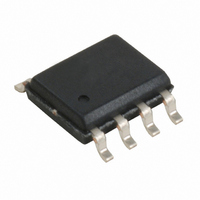
CY25560SXC Cypress Semiconductor Corp, CY25560SXC Datasheet - Page 6

CY25560SXC
Manufacturer Part Number
CY25560SXC
Description
IC CLOCK GEN 3.3V SS 8-SOIC
Manufacturer
Cypress Semiconductor Corp
Type
Clock/Frequency Synthesizer, Frequency Modulator, Spread Spectrum Clock Generatorr
Datasheet
1.CY25560SXC.pdf
(9 pages)
Specifications of CY25560SXC
Number Of Circuits
1
Package / Case
8-SOIC (3.9mm Width)
Pll
Yes
Input
Clock, Crystal
Output
Clock
Ratio - Input:output
1:1
Differential - Input:output
No/No
Frequency - Max
100MHz
Divider/multiplier
Yes/No
Voltage - Supply
2.97 V ~ 3.63 V
Operating Temperature
0°C ~ 70°C
Mounting Type
Surface Mount
Frequency-max
100MHz
Maximum Input Frequency
100 MHz
Minimum Input Frequency
25 MHz
Supply Voltage (max)
3.63 V
Supply Voltage (min)
2.97 V
Maximum Operating Temperature
+ 70 C
Minimum Operating Temperature
0 C
Mounting Style
SMD/SMT
Operating Supply Voltage
3.3 V
Lead Free Status / RoHS Status
Lead free / RoHS Compliant
Lead Free Status / RoHS Status
Lead free / RoHS Compliant, Lead free / RoHS Compliant
Other names
428-2222-5
CY25560SXC
CY25560SXC
Available stocks
Company
Part Number
Manufacturer
Quantity
Price
Company:
Part Number:
CY25560SXC
Manufacturer:
CY
Quantity:
1 262
Part Number:
CY25560SXC
Manufacturer:
CYP
Quantity:
20 000
Company:
Part Number:
CY25560SXCT
Manufacturer:
CYPRESS
Quantity:
1 710
Part Number:
CY25560SXCT
Manufacturer:
CYPRESS/赛普拉斯
Quantity:
20 000
Absolute Maximum Ratings
Commercial Grade
Supply Voltage (V
DC Input Voltage: ................................... –0.5V to VDD+0.5V
Junction Temperature ................................. –40°C to +140°C
Operating Temperature:...................................... 0°C to 70°C
Storage Temperature .................................. –65°C to +150°C
Static Discharge Voltage (ESD) ........................... 2,000V-Min
Table 3. DC Electrical Characteristics
V
Table 4. Electrical Timing Characteristics
V
Notes
Document #: 38-07425 Rev. *F
V
V
V
V
V
V
C
C
C
I
I
I
I
t
t
D
D
J
J
1. Operation at any Absolute Maximum Rating is not implied.
2. Single Power Supply: The voltage on any input or I/O pin cannot exceed the power pin during power up.
Parameter
Parameter
DD1
DD2
DD3
CLKFR
F
R
DD
DD
CC1
CC2
DD
IH
IM
IL
OH
OL
in1
in2
in2
TYin
TYout
= 3.3V±10%, T= 0°C to 70°C and C
= 3.3V±10%, T= 0°C to 70°C and C
Power Supply Range
Input High Voltage
Input Middle Voltage
Input Low Voltage
Output High Voltage
Output Low Voltage
Input Capacitance
Input Capacitance
Input Capacitance
Power Supply Current
Power Supply Current
Power Supply Current
Input Clock Frequency Range
Clock Rise Time (Pin 4)
Clock Fall Time (Pin 4)
Input Clock Duty Cycle
Output Clock Duty Cycle
Cycle-to-Cycle Jitter
Cycle-to-Cycle Jitter
DD
[1, 2]
):.....................................–0.5V to +6.0V
Description
Description
L
L
(Pin 4) = 15 pF, Unless Otherwise Noted
(Pin 4) = 15 pF, Unless Otherwise Noted
±10%
S0 and S1 only
S0 and S1 only
S0 and S1 only
I
I
Xin/CLK (Pin 1)
Xout (Pin 8)
S0, S1, SSCC (Pins 7, 6, 5)
FIN = 25 MHz, CL= 0
FIN = 65 MHz, CL= 0
FIN = 100 MHz, CL= 0
V
SSCLK at 0.4 – 2.4V
SSCLK at 0.4 – 2.4V
XIN/CLK (Pin 1)
SSCLK (Pin 4)
Fin = 25 MHz–50 MHz, SSCC = 1
Fin = 50 MHz–100 MHz, SSCC = 1
OH
OH
DD
= 6 mA
= 6 mA
= 3.30V
Conditions
Conditions
0.85V
0.40V
2.97
Min
Min
1.0
1.0
0.0
2.4
25
25
45
3
6
3
DD
DD
0.50V
Typ
V
Typ
150
130
1.8
1.8
3.3
0.0
42
50
50
17
27
4
8
4
DD
DD
0.60V
0.15V
Max
3.63
Max
V
100
300
200
0.4
2.8
2.8
10
23
41
59
75
55
5
5
DD
DD
DD
CY25560
Page 6 of 9
Unit
MHz
Unit
mA
mA
mA
pF
pF
pF
ns
ns
ps
ps
%
%
V
V
V
V
V
V
[+] Feedback


